I haven't really tested the contact bounce characteristics of any mechanical switch so I thought I'd use an oscilloscope to check those of an electromagnetic relay. I picked the
Telemecanique RXM2AB2JD mini relay with a 12VDC coil since I like that relay for its smart design and have a couple of them in stock.
Now we can't just use a mechanical switch to directly turn the relay on and off since that switch would itself have contact bounce. We need to switch the relay with a near perfect square wave. To make things simple I opted to use a 555 to perform this switching. I wired the 555 as a simple RS latch (flip flop) thus turning the 555 into a switch debouncer. So now we can use the any mechanical switch and the output of the 555 should, at least theoretically, be a clean, crisp, bounce-free square wave. Here's the debouncing circuit which I assembled on a solderless breadboard:
You will notice that pin2 is normally high while pin6 is normally low. When S(et) is pressed momentarily pin2 goes low and pin3 goes high and stays high. When R(eset) is momentarily pressed pin3 goes low and stays low.
Before showing the oscilloscope readings here's a guide to reading the Rigol DS1102E screen display.
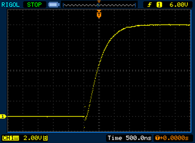
I tested the 555 output (pin 3) to make sure that I was getting a nice clean square wave. The following screenshot is a typical of what I got. As can be seen rise time is around 200ns while fall time is some 10x shorter.The oscilloscope was set to display dots (so we can see if sufficient samples were taken during the rise and fall).
I don't want the 555 getting loaded down by the moderately high current draw (~75mA @12VDC) of the relay so I used a 2N7000 MOSFET transistor to switch the relay coil. I checked the rise and fall times of 2N7000 as well just to make sure, so before installing the relay I connected a 10Kohm pull-up resistor to the transistor drain:
Here's the input-output voltage response diagram for the above circuits (555 with and without the 2N7000):
And here are the oscilloscope readings for V
O (voltage at transistor drain with respect to ground):
Below are the final test circuits with the relay and its normally open (NO) and normally closed (NC) contacts used for testing relay contact bounce. Star connections were used for V
CC and ground to try and isolate the control circuitry from relay coil noise produced during energization/de-energization.
The input-output response diagram:
The following screenshots show the voltage across the relay when it is switched on. Take note of the different time base of each shot. Each of them is a different acquisition (i.e., relay is switched off then turned on again for each screenshot). Ringing is conspicuous.
Below are screenshots showing the voltage across the relay when it is switched off. Again, take note of the different time bases of each shot, each of which is a different acquisition. Note as well that the vertical division is now 5VD/div in order to get all the data points on screen. As with turn-on ringing is evident.
In the following shot I wanted to show more detail of the relay voltage as it de-energizes so I decreased the vertical division to 2V/div. Time base is 100ns/div.
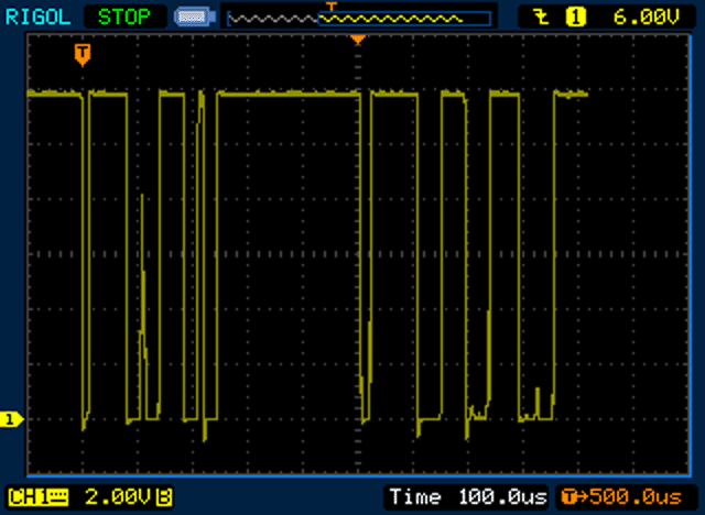
And finally, here are oscilloscope readings for the relay contact bounce.
A. Normally open contacts
1. N.O. contacts closing. For each the three acquisitions the waveform is presented first as a vector and followed by a screenshot showing it as dots. Note the differing time bases.
The following two shots are from the above 20µs acquisition. I merely dialed the time base up to 100µs (and hence we see the waveform is truncated at the right as the scope's sampling memory has been used up).
2. N.O. contacts opening. For each of the two acquisitions the waveform is presented first as a vector followed by a screenshot showing it as dots. Time base for both acquisitions is 20µs.
B. Normally closed contacts
1. N.O. contacts opening. For each of the three acquisitions the waveform is presented first as a vector followed by a screenshot showing it as dots. Note the differing time bases.
B. NC contacts closing. For each of the three acquisitions the waveform is presented first as a vector followed by a screenshot showing it as dots. The first three acquisitions have a time base of 500µs/div; the last two 50µs/div.
Summary
Contact bounce is clearly evident when the NO and NC contacts are closing, with the contacts closing and opening for many cycles before settling down to a steady closed position. From the readings above NO contact bounce period is from 2 to 2.5ms, while NC bounce is from 3 to 3.25ms. Compared to manual switches which may take tens of milliseconds to settle, contact bounce period of this relay is short.
NC contacts do not exhibit any bounce at all when opening. It's amazingly clean. NO contacts, however, show an interesting characteristic. There seems to be a short period (tens of microseconds to around 200ms) of high resistance--voltage across the contact (with reference to ground) hovers at around 3V. The resistance can be computed using the voltage divider rule for resistances in series.
Let
V
S = voltage source = 12V
R
1 = 10Kohm resistor
R
2 = NO contact resistance
V
R2 = voltage across R
2
V
R2 = R
2V
S / (R
1 + R
2)
Solving for R
2 we obtain:
R
2 = (V
R2R
1) / (V
S - V
R2)
Plugging in the values we obtain R
2 = 3.3Kohms
One possible reason for the difference in contact opening characteristic between NO and NC contacts is that NO opens under spring force while NC opens upon coil energization--the latter probably applies a much greater force than the spring thus greatly minimizing contact "sticking." Another reason could be arcing across the contacts while they're opening which is relatively slow under spring force. Contact opening characteristics will need to be further examined under higher voltages and currents.