Prototyping boards / stripboards are hardly the easiest way to make printed circuit boards. Because of the fixed pads and tracks it's impossible to optimize the layout, minimize board size, and eliminate the use of jumper wires to electrically join the components. In fact it's this latter "dis-feature" that drives me up the wall. Cutting short lengths of wire and soldering them onto the board is the kind of exasperating work that has made me stay away from making PCBs as much as I can. Personally I find it a pain in every part of the body using these boards. And for all the work the outcome is hardly pretty.
So graduating to "real" PCBs has been a relief. The only reason I've procrastinated is that when I tried Eagle years ago I just couldn't comprehend how to use it. Turns out that Eagle isn't the most intuitive EDA software. Kicad was another candidate recently, not least because it's freeware. But it made me tear my hair out as well. Fortunately I found one that's easy--almost fun--to use. DesignSpark PCB is completely free (for now at least) and has no restrictions on board size, layers, and other features. According to tests performed by some individuals, DS came out the winner amongst various EDAs (including Eagle and Kicad). I don't know how rigorous the tests were and how objective their assessment is, but personally I did find it relatively easy to get started. With DS I was able to produce my first PCB within a couple of days.
Apparently DS is a "non-crippled and modified version of Easy-PC." Moreover, another Easy-PC derivative, PCB Artist, is almost exactly the same as DS. What's so cool about the PCB Artist is that I've found a good number of video and pdf tutorials on their page. And practically all of what you can learn about PCB Artist applies directly to DS. Meanwhile, DS tutorials can be found right on software itself under the Help menu. At least one of the PCB Artist pdf tutorial is almost exactly the same as that of DS.
Most of the work in setting up DS will be customizing the component/schematic/pcb libraries. Even with the extensive number of parts from various manufacturers already in the libraries I've found myself adding more and more components and editing the pads of existing items in the pcb library. I've also realized that I waste a not insignificant amount of time shifting from one library to another so I'm copying the most often used components to my own library. I will be editing the schematic library as well--a lot of the symbols are not at all pretty.
Wednesday, March 30, 2011


Monday, March 14, 2011
Four-way traffic light

Not pretty at all. It looks worse than any signal light in Japan after it'd been felled and drowned by this week's Sendai tsunami. Good thing my nephew didn't mind its looks. Just hope it's strong enough to withstand the temblors from a 6-year old.
A Microchip PIC 12F1822 is the brains controlling the lights. To minimize power consumption its internal clock is set to just 125kHz. (This baby is capable of running at 32MHz!). Three AA batteries provide the juice. No current-limiting resistors are used for the LEDs. Measurements show they're not needed for VDD up to 4.5VDC. Only four MCU pins are used to switch the LEDs. Charlieplexing is employed to turn one LED in each of the four directions for 4milliseconds every 16 milliseconds (25% duty cycle). That's a frequency of around 62Hz--enough to fool the eye into not seeing the LEDs switching on and off that rapidly.
The original design was to power it off two AAs, but tests revealed that even without current limiting resistors the PIC could only deliver 5mA to the LEDs which have forward voltages of 1.6 to 1.8V. Considering the duty cycle is only 25% the average brightness would be quite low indeed. One option of course is to install very high brightness LEDs. I've searched RS Components and found various candidates. A possible drawback is that a number of these superbright LEDs have very high forward voltages, meaning their output will probably dramatically fall off as the batteries are depleted.
The circuit doesn't have an on/off (slide) switch. Instead the MCU goes to sleep 10 minutes after the last button press. When asleep pressing the button wakes it up and the light resumes operation in whatever it mode it was in when it dozed off.
When the lights are on the tactile switch/button allows the user to cycle between four modes:
1. Lights for opposite directions are on simultaneously. That is, when North-South is red, then South-North lights are red too and when NS is green SN is green too. Likewise with East-West and West East.
2. Light is green only in one direction at a time. This implies that for the direction that's green left-turning vehicles and those going straight can simultaneously go.
3. Four-way flashing yellow, 0.8 second on, 0.8 second off.
4. Four-way flashing red, 0.8 second on, 0.8 second off.
Just for fun I was tempted to add a four-way flashing green albeit at a much faster blink rate (say, 2 to 4 Hz). Would allow my nephews to have cars from all directions crashing into each other and getting a pile up. But I eventually scratched that idea--it's not a good way to train future drivers :)
Green stays on for 15 seconds, yellow for 2 seconds.
In modes 1 and 2, when after the light turns red, all directions will be red for a second. The rationale is that (in real life) any crazy driver beating the red light would be given enough time to cross the intersection without causing a tragedy.
When I gave the traffic light to John he critiqued the flashing mode saying one set should flashing yellow (eg. NS and SN) while the other (eg. EW and WE) should be flashing red. Actually I can't remember which lights are on in real four-way traffic lights during flashing mode. Googling shows that my nephew has a point. That's trivial enough to implement, given that the firmware uses a state machine implementation to charlieplex the lights.


The table on the right shows which lines (PORT pins) control which traffic light direction. The table on the left gives the TRIS and PORT status in order to light up LED Lx.
Here's the light at work:
Hoping to make a much more decent model the next time around.
Wednesday, March 2, 2011
PIC 12F1822 current draw at different frequencies
Because the datasheet for the PIC 12F1822 lists the supply current for only a select number of internal oscillator frequencies I went and measured the current draw for all of them under various I/O settings.
The MCU was programmed and powered by a PICkit2 whose VDD was set to 5.0VDC when programming. It was set to either 5.0V or 3.0V when logging maximum, minimum and average current draw. The only thing connected to the MCU was the PICkit 2. The two were mated throughout the test. No resistors, capacitors, etc. were used. Ambient temperature during tests was 27° to 29° Celsius.
A Fluke 87V digital multimeter was set to read µA, with Min-Max feature enabled. The DMM was hooked up in series with the MCU's VSS and PICkit2's VSS. The meter was given between half a minute to a minute to gather data.
In the MCU configuration words, INTOSC with I/O function on CLKIN pin was selected. MCLRE, WDTE and PLLEN were disabled. Note that with the MCLR inoperative, RA3/MCLR pin is floating. Leaving an input floating increases current draw. In the tests below weak pull-ups were either enabled or disabled to record this difference. All peripherals (ADC, comparators, etc.) were left at their default settings, which I believe are off.
The various firmware used are provided below. C compiler employed was the mikroC Pro v4.60
A1.
A2.
B1.
B2.
C1.
C2.
Open this Google spreadsheet to see the test results. As can be clearly seen, the lowest power consumption is obtained with I/O pins set as output. The worst configuration as expected is that with floating inputs. It was discovered that having analog instead of digital inputs just slightly decreases current draw.
Below are screenshots of the pertinent table from the datasheet:


Compared to the datasheet, the results I obtained shows the 12F1822 (at least the chip I tested) performs better than specification, although I hardly duplicated Microchip's test conditions exactly.
According to the specs the LF version draws a maximum of 1.1µA during sleep @85°C, compared to the F version's 45µA. The astronomical difference probably implies the F version employs a low drop out voltage regulator to supply the MCU core with 3.6V (see the datasheets for the PIC 16F193X series for notes on the LDO).
The MCU was programmed and powered by a PICkit2 whose VDD was set to 5.0VDC when programming. It was set to either 5.0V or 3.0V when logging maximum, minimum and average current draw. The only thing connected to the MCU was the PICkit 2. The two were mated throughout the test. No resistors, capacitors, etc. were used. Ambient temperature during tests was 27° to 29° Celsius.
A Fluke 87V digital multimeter was set to read µA, with Min-Max feature enabled. The DMM was hooked up in series with the MCU's VSS and PICkit2's VSS. The meter was given between half a minute to a minute to gather data.
In the MCU configuration words, INTOSC with I/O function on CLKIN pin was selected. MCLRE, WDTE and PLLEN were disabled. Note that with the MCLR inoperative, RA3/MCLR pin is floating. Leaving an input floating increases current draw. In the tests below weak pull-ups were either enabled or disabled to record this difference. All peripherals (ADC, comparators, etc.) were left at their default settings, which I believe are off.
The various firmware used are provided below. C compiler employed was the mikroC Pro v4.60
A1.
// FOR MEASURING CURRENT AT VARIOUS INTERNAL OSCILLATOR FREQUENCIES
// All I/O pins are all digital outputs in sinking current mode (grounded)
// RA3/MCLR pin weak pull-up is enabled (MCU automatically disables pull ups for pins configured as output)
void main()
{
  PORTA = 0;
  TRISA = 0;
  ANSELA = 0;
  NOT_WPUEN_bit = 0;    // global pull-up enable
  WPUA = 0XFF;          // individual pull-up enable
  OSCCON = 0b0;         // change OSCCON value to set various internal oscillator frequencies
  while(1) ;
}
A2.
// FOR MEASURING SLEEP CURRENT
// All I/O pins are all digital outputs in sinking current mode (grounded)
// RA3/MCLR pin weak pull-up is enabled (MCU automatically disables pull ups for pins configured as output)
void main()
{
  PORTA = 0;
  TRISA = 0;
  ANSELA = 0;
  NOT_WPUEN_bit = 0;    // global pull-up enable
  WPUA = 0XFF;          // individual pull-up enable
  asm sleep
  while(1) ;
}
B1.
// FOR MEASURING CURRENT AT VARIOUS INTERNAL OSCILLATOR FREQUENCIES
// All I/O pins are by default analog inputs
// All weak pull-ups are enabled
void main()
{
  NOT_WPUEN_bit = 0;    // global pull-up enable
  WPUA = 0XFF;          // individual pull-up enable
  OSCCON = 0b0;         // change OSCCON value to set various internal oscillator frequencies
  while(1) ;
}
B2.
// FOR MEASURING SLEEP CURRENT
// All I/O pins are by default analog inputs
// All weak pull-ups are enabled
void main()
{
  NOT_WPUEN_bit = 0;    // global pull-up enable
  WPUA = 0XFF;          // individual pull-up enable
  asm sleep
  while(1) ;
}
C1.
// FOR MEASURING CURRENT AT VARIOUS INTERNAL OSCILLATOR FREQUENCIES
// All I/O pins are by default analog inputs
// All weak pull-ups are by default disabled
void main()
{
  OSCCON = 0b0;         // change OSCCON value to set various internal oscillator frequencies
  while(1) ;
}
C2.
// FOR MEASURING SLEEP CURRENT
// All I/O pins are by default analog inputs
// All weak pull-ups are by default disabled
void main()
{
  asm sleep
  while(1) ;
}
Open this Google spreadsheet to see the test results. As can be clearly seen, the lowest power consumption is obtained with I/O pins set as output. The worst configuration as expected is that with floating inputs. It was discovered that having analog instead of digital inputs just slightly decreases current draw.
Below are screenshots of the pertinent table from the datasheet:


Compared to the datasheet, the results I obtained shows the 12F1822 (at least the chip I tested) performs better than specification, although I hardly duplicated Microchip's test conditions exactly.
According to the specs the LF version draws a maximum of 1.1µA during sleep @85°C, compared to the F version's 45µA. The astronomical difference probably implies the F version employs a low drop out voltage regulator to supply the MCU core with 3.6V (see the datasheets for the PIC 16F193X series for notes on the LDO).
Friday, February 18, 2011
Now when will I get one?
Agilent just unveiled its latest lines of InfiniiVision oscilloscopes. Brochure and spec sheet for the 2000X and 3000X. Dave Jones has a comprehensive review of this wonderful, jaw dropping scope.
Monday, February 7, 2011
Philips RC-5 Infrared Protocol Decoding
Currently developing a circuit that will have as its input device off-the-shelf (TV) remote controls. I initially planned on using the NEC protocol given its inclusion of the complement of the command code which could be used for signal/data integrity checking. However, given that each NEC frame has 32 bits + a leader code (start bit), I decided to use the simpler and less interrupt-service-routine-intensive RC5 protocol by Philips.
The following will be a primer on the method I'm using to decode the RC5 signal. The IR receiver I used for the circuit is the Osram SFH5110-38. This particular part is suppose to be used for IR signals with a 38kHz carrier frequency, but the Philips uses 36kHz. Tests show the Osram has no problem picking up the Philips transmission although I cannot say what improvement in quality of signal output (particularly bit periods) will be if a 36kHz receiver is employed. For the remote control I used a Cybertec RM-312x universal control programmed with setup code 1528 for Philips TV.
Introduction
The Philips RC5 uses bi-phase encoding whereby:
Here's a summary of the RC5 protocol (this image is purportedly from an original 1992 Philips document on the RC5).

One RC5 bit period = 1.778ms. Half of that is 0.889ms. The start bit is always a logic one and occurs, of course, at the middle of the first bit period. The entire RC5 word is repeated every 114ms while the remote control key is kept pressed. The Toggle/ Control bit remains at the same logic level as long the present key is not released. This bit will toggle if the key is released and another key is pressed or the same key is pressed. The Toggle/Control bit can therefore be used to detect whether the current key is still pressed (required for instance for TV volume control) or the same key has been released and pressed again (required for the input of digits for example).
The above diagram is from the point of view of the IR transmitter wherein the IR LED is normally off (to conserve battery power). The IR receiver output, however, is normally on (output voltage is high while no IR signal is detected). Because of this the output of the receiver will be the complement of the transmitted signal and thus:
The receiver has circuitry to filter out the 36kHz carrier wave and thus its output is clean and doesn't have the 36kHz "spikes."
From the point of view of the IR receiver output here are some important facts we can infer from the RC5 protocol:
MCU Implementation
The test circuit consisted of a Microchip PIC16F883 microcontroller using its internal RC clock running at 4MHz, an Osram SFH5110-38 infrared receiver, and four discrete LEDs as indicators to see if the IR signal was being detected and whether the transmitted command codes were being correctly decoded. The circuit was powered by an ATX supply since I discovered via oscilloscope that the PICkit 2 apparently didn't have enough juice to power the IR receiver--even with a 1uF tantalum or 10uF aluminum cap at the VS pin of the IR receiver its output would sporadically spike down to low (zero volts) even with no signal being received. And when signal was received its output was garbage.
Because level changes (falling and rising edges) need to be detected the output pin of the IR receiver is connected to an MCU pin that has interrupt-on-change (IOC) capability. In this case I chose the 883's RB0 pin. With the proper special function registers (SFR) set up, an interrupt will occur whenever a level change occurs--whenever voltage at the RB0 changes from high to low or from low to high.
A timer is set up so the elapsed time between successive IOCs can be measured. If it's ~0.889ms then we know half a bit period has passed. If it's ~1.778ms then elapsed time is a full bit period. I used Timer0 with a prescaler value of 1:16. Given the 1µs instruction cycle, register TMR0 will overflow every 256 x 16 x 1µs = 4.096ms (INTCON.T0IF will be set even if interrupt is not enabled).
The start of a RC5 word is the first falling edge detected after the IR receiver has been high for over 4.096ms--when Timer0 overflows and its interrupt flag gets set. This falling edge indicates the start bit. The start bit is not recorded/stored. It is used only as the reference for determining the middle of the bit periods. This falling edge occurs at the middle of the first bit period of the word, so every full bit period (1.778ms) after this is the middle of a bit period.
When an IOC occurs and the measured elapsed time from the last IOC is half a bit period long, given there was no prior half bit period or the previous half bit period has already been paired, then according to F3 the very next IOC will occur after half a bit period. That will then be the middle of a bit period. Checking the direction of the level change provides the bit value. Alternately, as per F4 that bit will have the same value as the previous bit.
When an IOC occurs and the measured elapsed time from the last IOC is a full bit period then the current IOC has occured at the middle of a bit period and the bit value (0 or 1) is recorded, depending on the direction of the level change. Because of F5, instead of checking the direction of level change, the value of current bit can be obtained by looking at the value of the previous bit.
Because the RC5 word is transmitted MSB first, we left shift the incoming bits into their storage variables (registers). Because I will be using the Command codes and the Control bit but won't for now be using the Address bits I've decided to store the Command bits in one variable and the rest in another.
As the Field bit, Control bit, and 5-bit System Address are received they are left-shifted into variable RC5FCSYS. Thus when all the bits are in, the Field bit and Control bit will be in bits 6 and 5 of RC5FCSYS, respectively, and the MSB and LSB of the System Address will be in bits 4 and 0 of RC5FCSYS, respectively.
The 6-bit Command bits are left-shifted into RC5COMM in the order they are received by the IR receiver. Thus, after all the bits are in, the MSB and LSB of the Command code will be in bits 5 and 0, respectively.
Variable RC5BITS keeps track of the number of bits already received and is used to determine into which of the two variables the current bit will be stored.
Because the bit period of the incoming signal will never be exactly as per specifcation and because the MCU is running on its internal RC clock with limited accuracy, we need to predetermine a range of incoming IR pulse widths that are accepted as legitimate half and full bit periods. Any received pulse width outside these ranges will be considered an indication of an error and the entire RC5 word will be disregarded.
An oscilloscope can be used to sample several half and full bit periods from various remote controls (IR transmitters) used at various distances from the IR receiver. The Cybertec remote control used to test the firmware had half bit periods that were within ±20% and full bit periods within ±10%. Using 20% the ranges are: half bit period: 0.7112ms to 1.0668ms, full bit period: 1.4224ms to 2.1336ms. Those values were converted to 8-bit integers taking into account the MCU clock frequency and timer prescale value.
After the firmware had been debugged, the response of the MCU to IR signals was found to be unreliable and intermittent--there was noticeable inability to detect valid signals around 50% of the time. So I increased the tolerance to ±25%. Thus the acceptable ranges of values increased to 0.66675 to 1.11125ms and 1.3335 to 2.2225ms. With that increased range the MCU picked up the transmission every time. Transmitter was tested up to 4 meters and within 45degrees of the receiver (zero degrees is perpendicular to the face of the receiver).
Note that if tolerance is uniform for both upper and lower limits and for half and full bit periods then the maximum tolerance allowable is 33% since with a value >33% the half bit period upper limit will be greater than the full bit period lower limit: 0.889ms + 0.889x > 1.778ms - 1.778x, with x > 1/3. Tolerances needn't be uniform, of course. If, as with the Cybertec remote control, the full bit period tolerances are much better than the half bit period's, then the range for the full bit period can be decreased accordingly.
Here's the pertinent part of the RC5 decoding firmware. It was written in mikroC Pro for PIC.
----
References:
AN10210 Using the Philips 87LPC76x microcontroller as a remote control transmitter
Philips RC-5 Protocol
The following will be a primer on the method I'm using to decode the RC5 signal. The IR receiver I used for the circuit is the Osram SFH5110-38. This particular part is suppose to be used for IR signals with a 38kHz carrier frequency, but the Philips uses 36kHz. Tests show the Osram has no problem picking up the Philips transmission although I cannot say what improvement in quality of signal output (particularly bit periods) will be if a 36kHz receiver is employed. For the remote control I used a Cybertec RM-312x universal control programmed with setup code 1528 for Philips TV.
Introduction
The Philips RC5 uses bi-phase encoding whereby:
- logic zero is represented by a falling edge during the middle of the bit period
- logic one is represented by a rising edge during the middle of the bit period
Here's a summary of the RC5 protocol (this image is purportedly from an original 1992 Philips document on the RC5).

One RC5 bit period = 1.778ms. Half of that is 0.889ms. The start bit is always a logic one and occurs, of course, at the middle of the first bit period. The entire RC5 word is repeated every 114ms while the remote control key is kept pressed. The Toggle/ Control bit remains at the same logic level as long the present key is not released. This bit will toggle if the key is released and another key is pressed or the same key is pressed. The Toggle/Control bit can therefore be used to detect whether the current key is still pressed (required for instance for TV volume control) or the same key has been released and pressed again (required for the input of digits for example).
The above diagram is from the point of view of the IR transmitter wherein the IR LED is normally off (to conserve battery power). The IR receiver output, however, is normally on (output voltage is high while no IR signal is detected). Because of this the output of the receiver will be the complement of the transmitted signal and thus:
- logic zero is represented by a rising edge
- logic one is represented by a falling edge
The receiver has circuitry to filter out the 36kHz carrier wave and thus its output is clean and doesn't have the 36kHz "spikes."
From the point of view of the IR receiver output here are some important facts we can infer from the RC5 protocol:
- F1. A level change must occur during the middle of every bit period.
- F2. A level change may or may not occur during the start/end of a bit period.
- F3. Half-bit-period level changes (i.e., the elapsed time between two level changes is 0.889ms) always occur in pairs, with the latest/current level change occurring at the middle of a bit period.
- F4. Given a pair of half-bit-period level changes, the current bit has the same value as the previous bit, i.e., if the value of previous bit was a logic one then the value of the current bit is a logic one, and the current bit is a logic zero if the previous bit was a logic zero.
- F5. Given a full-bit-period level change (i.e., the elapsed time between two level changes is 1.778ms), the current level change occurred at the middle of a bit period, and the value of the current bit will be the complement of the value of the previous bit, i.e., if the previous bit was a logic one then the current bit is a logic zero, and the current bit is a logic one if the previous bit was a logic zero.
MCU Implementation
The test circuit consisted of a Microchip PIC16F883 microcontroller using its internal RC clock running at 4MHz, an Osram SFH5110-38 infrared receiver, and four discrete LEDs as indicators to see if the IR signal was being detected and whether the transmitted command codes were being correctly decoded. The circuit was powered by an ATX supply since I discovered via oscilloscope that the PICkit 2 apparently didn't have enough juice to power the IR receiver--even with a 1uF tantalum or 10uF aluminum cap at the VS pin of the IR receiver its output would sporadically spike down to low (zero volts) even with no signal being received. And when signal was received its output was garbage.
Because level changes (falling and rising edges) need to be detected the output pin of the IR receiver is connected to an MCU pin that has interrupt-on-change (IOC) capability. In this case I chose the 883's RB0 pin. With the proper special function registers (SFR) set up, an interrupt will occur whenever a level change occurs--whenever voltage at the RB0 changes from high to low or from low to high.
A timer is set up so the elapsed time between successive IOCs can be measured. If it's ~0.889ms then we know half a bit period has passed. If it's ~1.778ms then elapsed time is a full bit period. I used Timer0 with a prescaler value of 1:16. Given the 1µs instruction cycle, register TMR0 will overflow every 256 x 16 x 1µs = 4.096ms (INTCON.T0IF will be set even if interrupt is not enabled).
The start of a RC5 word is the first falling edge detected after the IR receiver has been high for over 4.096ms--when Timer0 overflows and its interrupt flag gets set. This falling edge indicates the start bit. The start bit is not recorded/stored. It is used only as the reference for determining the middle of the bit periods. This falling edge occurs at the middle of the first bit period of the word, so every full bit period (1.778ms) after this is the middle of a bit period.
When an IOC occurs and the measured elapsed time from the last IOC is half a bit period long, given there was no prior half bit period or the previous half bit period has already been paired, then according to F3 the very next IOC will occur after half a bit period. That will then be the middle of a bit period. Checking the direction of the level change provides the bit value. Alternately, as per F4 that bit will have the same value as the previous bit.
When an IOC occurs and the measured elapsed time from the last IOC is a full bit period then the current IOC has occured at the middle of a bit period and the bit value (0 or 1) is recorded, depending on the direction of the level change. Because of F5, instead of checking the direction of level change, the value of current bit can be obtained by looking at the value of the previous bit.
Because the RC5 word is transmitted MSB first, we left shift the incoming bits into their storage variables (registers). Because I will be using the Command codes and the Control bit but won't for now be using the Address bits I've decided to store the Command bits in one variable and the rest in another.
As the Field bit, Control bit, and 5-bit System Address are received they are left-shifted into variable RC5FCSYS. Thus when all the bits are in, the Field bit and Control bit will be in bits 6 and 5 of RC5FCSYS, respectively, and the MSB and LSB of the System Address will be in bits 4 and 0 of RC5FCSYS, respectively.
The 6-bit Command bits are left-shifted into RC5COMM in the order they are received by the IR receiver. Thus, after all the bits are in, the MSB and LSB of the Command code will be in bits 5 and 0, respectively.
Variable RC5BITS keeps track of the number of bits already received and is used to determine into which of the two variables the current bit will be stored.
Because the bit period of the incoming signal will never be exactly as per specifcation and because the MCU is running on its internal RC clock with limited accuracy, we need to predetermine a range of incoming IR pulse widths that are accepted as legitimate half and full bit periods. Any received pulse width outside these ranges will be considered an indication of an error and the entire RC5 word will be disregarded.
An oscilloscope can be used to sample several half and full bit periods from various remote controls (IR transmitters) used at various distances from the IR receiver. The Cybertec remote control used to test the firmware had half bit periods that were within ±20% and full bit periods within ±10%. Using 20% the ranges are: half bit period: 0.7112ms to 1.0668ms, full bit period: 1.4224ms to 2.1336ms. Those values were converted to 8-bit integers taking into account the MCU clock frequency and timer prescale value.
After the firmware had been debugged, the response of the MCU to IR signals was found to be unreliable and intermittent--there was noticeable inability to detect valid signals around 50% of the time. So I increased the tolerance to ±25%. Thus the acceptable ranges of values increased to 0.66675 to 1.11125ms and 1.3335 to 2.2225ms. With that increased range the MCU picked up the transmission every time. Transmitter was tested up to 4 meters and within 45degrees of the receiver (zero degrees is perpendicular to the face of the receiver).
Note that if tolerance is uniform for both upper and lower limits and for half and full bit periods then the maximum tolerance allowable is 33% since with a value >33% the half bit period upper limit will be greater than the full bit period lower limit: 0.889ms + 0.889x > 1.778ms - 1.778x, with x > 1/3. Tolerances needn't be uniform, of course. If, as with the Cybertec remote control, the full bit period tolerances are much better than the half bit period's, then the range for the full bit period can be decreased accordingly.
Here's the pertinent part of the RC5 decoding firmware. It was written in mikroC Pro for PIC.
/*

Philips RC5 Decoding Routine
February 2011
Edwardson Tan
processor = PIC16F883
*/

#define  irr                 PORTB.f0  // Osram SFH5110-38 infrared receiver
#define  tris_irr            TRISB.f0  // for use with setting the appropriate pin as input

// RC5 decoding defines
#define  rc5_on              FEN.f0              // 1 = irr output has been high for >4millisec and then goes low; this indicates a RC5 start bit
                                                 // 0 = irr output has been low for >4millisec and then goes high. This is an abnormal state and is an error
                                                 // rc5_on is also reset to 0 when all bits of word have been received
#define  halfper_prev        FEN.f1              // 1 = the last IOC was a half bit period, 0 = the last IOC occured after a full bit period
#define  button_pressed      FEN.f2              // 1 = button has been pressed and valid RC5 word stored
#define rc5_read_error FEN.f3 // 1 = read error, pulse width of either a zero or one bit is outside the acceptable limits; the data packet should be discarded
#define bit_period FEN.f4 // _full = 1 = one full bit period, _half = 0 = half bit period
#define curr_bit FEN.f5 // contains the latest decoded value of the bit of the RC5 word being received
#define _full 1
#define _half 0
// one full bit period for RC5 = 1.778ms; one half bit period = 0.889ms
// given clock = 4MHz and TMR0 initial value = 0 and timer0 prescale = 1:16, TMR0 overflows every 256 x 16 / 1MHz = 4.096ms
// 4.096ms / TMR0 count = 4.096 / 256 = 0.016ms per TMR0 count
// 1.778 / 0.016ms = 111 this is the TMR0 count when time elapsed is 1.778ms
#define _fullbit 111 // full bit period of RC5
#define _tolerance 25 // tolerance in percent, to be added/subtracted to/from half and full bit periods to create range of acceptable pulse widths
// !! THIS HAS TO BE INTEGER NOT FLOATING POINT !!
// !! MAXIMUM VALUE = 33%, ELSE halfbit_uplim WILL BE GREATER THAN fullbit_uplim
#define _halfbit _fullbit / 2 // half bit period of RC5
#define halfbit_lolim _halfbit - (_halfbit * _tolerance / 100) // minimum pulse duration for half bit period
#define halfbit_uplim _halfbit + (_halfbit * _tolerance / 100) // maximum pulse duration for half bit period
#define fullbit_lolim _fullbit - (_fullbit * _tolerance / 100) // minimum pulse duration for full bit period
#define fullbit_uplim _fullbit + (_fullbit * _tolerance / 100) // maximum pulse duration for full bit period
// ===========================================================================================
// Global Variables
// ===========================================================================================
int8 FEN = 0; // Flag and ENable and status bits register
int8 PULSEWIDTH; // contains the measured pulse width (to get the real value in millisec multiply by 16)
int8 RC5BITS; // contains the bit number (excluding the start bit) of the RC5 word currently being received
int8 RC5FCSYS; // contains the RC5 Field bit, Control Bit, and the 5-bit System Address
int8 RC5COMM; // contains the RC5 6-bit Command code
int8 TEMP; // temporary memory
// ===========================================================================================
// Functions
// ===========================================================================================
void InitRegisters()
{
PORTA = 0;
PORTB = 0;
PORTC = 0;
TRISA = 0;
TRISB = 0;
TRISC = 0;
ANSEL = 0;
ANSELH = 0;
tris_irr = 1;
OPTION_REG = 0b10000011; // prescaler assigned to timer0
// prescale = 1:16
// timer0 uses internal clock instruction cycle
// weak pull ups disabled
// enable interrupt on change
// intialize RB0/INT pin to interrupt on input change -- pin is connected to IR receiver
INTCON.RBIE = on;
IOCB = 0b1;
INTCON.GIE = 1;
INTCON.PEIE = 1;
} // void InitRegisters()
// ===========================================================================================
// ISR
// ===========================================================================================
void interrupt()
{
// interrupt on change
if (INTCON.RBIF)
{
PULSEWIDTH = TMR0;
TMR0 = 0;
TEMP = PORTB; // a read of PORTB is necessary before RBIF can be cleared
INTCON.RBIF = 0;
if (rc5_on && !rc5_read_error)
{
if (PULSEWIDTH >= halfbit_lolim && PULSEWIDTH <= halfbit_uplim)
bit_period = _half;
else if (PULSEWIDTH >= fullbit_lolim && PULSEWIDTH <= fullbit_uplim)
bit_period = _full;
else
rc5_read_error = 1;
if (bit_period == _half && halfper_prev == 0)
{
halfper_prev = 1; // last IOC occured after a full bit period, so this current half bit period needs to be paird with the half bit period
}
else // if (bit_period == _full || halfper_prev == 1)
{
halfper_prev = 0;
if (irr) // rising edge, indicates logic zero
curr_bit = 0;
else // falling edge, indicates logic one
curr_bit = 1;
if (RC5BITS <= 6)
{
RC5FCSYS <<= 1;
RC5FCSYS.f0 = curr_bit;
}
else
{
RC5COMM <<= 1;
RC5COMM.f0 = curr_bit;
}
if (++RC5BITS >=13)
{
rc5_on = 0;
button_pressed = 1;
}
}
} // if (rc5_on && !rc5_read_error)
// if timer0 interrupt flag is set then ir_rx output was low/high for >4ms before the IOC that just occurred
if (INTCON.T0IF)
{
INTCON.T0IF = 0;
RC5BITS = 0;
RC5FCSYS = 0;
RC5COMM = 0;
rc5_read_error = 0;
rc5_on = 0;
if (!irr) // falling edge; pulse was high for >4ms so this is considered the start bit of RC5 word
rc5_on = 1;
}
} // if (INTCON.RBIF)
} // void interrupt()
----
References:
AN10210 Using the Philips 87LPC76x microcontroller as a remote control transmitter
Philips RC-5 Protocol
Monday, January 24, 2011
99-minute timer with dual 7-segment LED display

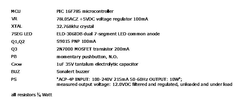
My objective in this design was to simply it as much as possible parts-wise--to minimize the number of discretes. The original design called for the use of MOSFET transistors exclusively to obviate the need for base resistors but I currently don't have any common cathode LED displays on hand and I need a timer ASAP so I had to use PNPs for the common anode display. There is only one pushbutton and it uses the weak pull-up of the MCU, hence a discrete pull-up resistor is unnecessary.
Features:
- Maximum time/readout = 99 minutes
- Display is shut down and MCU goes to sleep 10 seconds after readout becomes zero
- After timing has commenced readout flashes at a frequency of exactly 1Hz and with a duty cycle of 50%. Flashing readout is therefore counting down seconds.
- The pushbutton has multiple functions depending on status of the timer:
- when readout is on, pressing it for a fraction of a second increments readout by one. Keeping it depressed for half a second increments readout by 10 and keeps incrementing by 10 while pressed. No further readout change will occur when readout rolls over to zero. Button must be released and depressed again to increment again.
- when readout is off (MCU is in sleep mode) button acts to wake up the MCU.
- when timer has begun countdown but has not yet reached zero, button acts to abort timing.
- when timer has counted down to zero and buzzer alert is sounding, button acts to stop the buzzer
Detailed description of timer operation and its firmware:
Upon power up, the MCU will be in Standby mode and 2-digit seven-segment LED display will read 0. If PB is momentarily pressed a 7ms beep will sound and the LED display will read 1. Because of the limitations of the display, the maximum number of minutes the system will accommodate is 99 minutes.
After the first keypress (unless it was to awaken the MCU) firmware enters Userinputting mode. Further momentary presses of PB will increment the time by one and a 7ms beep will sound and time will be displayed. Keeping PB depressed for about half a second will increment time by 10 minutes. If time displayed is not a multiple of ten (ie., dividing by ten will result in a remainder), then keeping PB pressed will change time to the next nearest higher multiple of 10. Eg. If current time displayed = 8 then it will be changed to 10. If display = 24 then it will be changed to 30. If PB is kept depressed, increment by 10 will continue until the key is released or until time increments to 0 (there is no 100). A 7ms beep will sound every time heating time is incremented/decremented by 10.
If time displayed is not zero then after no button presses are made for approx 3 seconds from the last button press, countdown will begin and four sets of 50ms beep followed by 50ms silence will sound to indicate that countdown has commenced. Firmware is now in Countingdown mode. The amount of time left will be displayed and display will flash once every second. When time is down to 1 minute, display will change from displaying minutes to seconds. Thus at one minute it will display "60" meaning 60 seconds. Display will cease flashing. Pressing either button while in Countingdown mode will abort countdown and a 7ms beep will sound. Firmware is then returned to Standby mode.
When countdown time has elapsed firmware is changed to Countdownfinished mode. 3 alarm sequences are sounded in succession: 10 sets of 0.1sec beep + 2sec silence, 10 sets of 0.25sec beep + 1.25sec silence, continuous 0.5sec beep + 0.5sec silence. At any time when firmware is in Countdownfinished mode, any button press will terminate the alarm and firmware will be switched back to Standby mode.
When in Standby mode and no button presses are received in approx 10 seconds, LED display is turned off and the MCU goes to sleep. It can be awakened by a button press. The button press that awakes the MCU does not count as time input--the reading is zero when the MCU wakes up. No beep is sounded when a button press wakes up the MCU.
Timer0 is set up to overflow every 8ms. In main() timer0 interrupt flag is continually polled. When it gets set, the input button is checked by the switch debounce routine. This routine determines whether the switch is bouncing or not, and if not whether it is at a high/low level and whether or not a falling/rising edge has occured. A falling edge indicates a valid button press. The routine also keeps track of how long the button has remained pressed and how long it has remained not pressed.
Timer1 is used for countdown timing. Timer1 uses an external 32.768kHz crystal for its clock. With a prescale set to 1:1, TMR1L = 0, and TMR1H set to 192, timer1 overflows every 256 * 64 / 32768 = 0.5sec. Timer1 is turned on only when countdown commences and is stopped after countdown or an aborted countdown.
Firmware uses a state machine implemented using switch()/case statement. There are four possible states: Standby, Userinputting, Countingdown, and Countdownfinished. Upon power up state = Standby. After any button press state changes over to Userinputting. Should countdown commence state changes to Countingdown. Should inputting be canceled states changes to Standby. Upon completion of countdown state changes over to Countdownfinished. When a button is pressed to stop alarm state changes to Standby.
The two digits of the seven segment display are multiplexed and each digit is turned on every time timer0 overflows (8ms). Thus, the refresh rate is 62.5Hz. Because of display flickering problem button beep should be less than timer0 overflow period. When longer beeps are required (eg. to indicate countdown has ended) a state machine implementation (employing switch()/case statement) is used within the main state machine.
Watchdog timer is enabled when MCU is awake and disabled when it goes to sleep. PORTA pull up for input button is enabled. Button is debounced in software. When MCU goes to sleep interrupt-on-change is enabled to allow button press to wake up the MCU. Upon waking IOC is disabled.
Wednesday, January 5, 2011
555 propagation delay
Still using the same 555-relay circuit I did a "prequel" and monitored the propagation delay between S(et)-R(eset) inputs and 555 output state change. Channel 1 of oscilloscope was connected to either pin2 or pin6 of the 555, while channel two was connected to pin3. Ground clips were connected to circuit ground. Trigger mode was of course single sweep, rising or falling edge triggered, and triggering on channel 1. Trigger voltage was adjusted accordingly depending on whether rising or falling edge trigger was selected. Each screenshot below is a different, unique acquisition.
The switch used for S and R were simply short lengths of AWG#22 solid wire. One end was plugged into the breadboard slot for pin2/pin6 and the other end was momentarily plugged into the ground/VCC slot when the 555 was to be triggered. What amazed me--and as you will see in the shots below--was that there was no contact bounce at all with this most primitive method of switching.
A. Channel 1: 555 pin2, falling edge trigger.
Propagation delay, measured @50% of VCC: ~200ns


B. Channel 1: 555 pin6, rising edge trigger
Propagation delay, measured @50% of VCC: ~175ns


Interestingly, there's very noticeable ringing when pin3 goes from high to low. And it begins the moment pin6 goes high. Quite intriguing. Wonder what's happening internally.
All of the tests above were done with the 2N7000 and relay connected. They were disconnected from the circuit and the results were still the same including the observed pin3 ringing.
The switch used for S and R were simply short lengths of AWG#22 solid wire. One end was plugged into the breadboard slot for pin2/pin6 and the other end was momentarily plugged into the ground/VCC slot when the 555 was to be triggered. What amazed me--and as you will see in the shots below--was that there was no contact bounce at all with this most primitive method of switching.
A. Channel 1: 555 pin2, falling edge trigger.
Propagation delay, measured @50% of VCC: ~200ns


B. Channel 1: 555 pin6, rising edge trigger
Propagation delay, measured @50% of VCC: ~175ns


Interestingly, there's very noticeable ringing when pin3 goes from high to low. And it begins the moment pin6 goes high. Quite intriguing. Wonder what's happening internally.
All of the tests above were done with the 2N7000 and relay connected. They were disconnected from the circuit and the results were still the same including the observed pin3 ringing.
Subscribe to:
Posts (Atom)