In any automatic night light circuit that's meant to switch on perimeter security lights, the time period we are most interested in is dusk and dawn. We want the lights to be switched on at dusk and turned off at dawn. (Whether the lights are turned on/off earlier or later is dependent on the user.) During the night we want the lights on regardless of lightning flashes or car headlamps shining on the sensor or bright city lights being reflected by the clouds or a full moon or what have you. During the daytime we want the lights off regardless of clouds rolling in and out and thus momentarily blocking the sun, or a very overcast day, or a heavy downpour. Of course we would want the lights turned on even during the middle of the day if for some reason utter darkness descended such as during a (near) total solar eclipse, or--if we wanted to test the circuit--if we covered the sensor with some opaque material.
I've discussed the following light sensor here and here. Just a summary of how it works: R1 and LDR form a voltage divider. When the voltage across LDR is greater than across the 10uF capacitor, the cap gets charged via D1. When voltage across the cap is greater than across LDR, the capacitor discharges via R2. Given how D1 shunts R2 during charging and given that R1 has a much lower value than R2, the net result is that charging rate is faster than discharge rate. This means that when there is an abrupt and large increase in the level of ambient light (LDR resistance decreases) the voltage across the cap decreases slower compared to when there is sudden and large decrease in light level (LDR resistance increases). In other words, the circuit has a greater inertia to positive changes in light level than to negative changes in light level. During daytime, assuming the sensor were located outdoors and were we to shroud it with a black opaque bag, the voltage output would within seconds rise close to VDD. Were we then to take off the bag, the voltage would drop back to near ground level but a slower rate than when darkness fell upon the LDR.
Recently I provided an update on the MCU-based ANLC I'm testing. It's still a work in progress but I thought I'd provide more information on the algorithm I'm using to try and mimic the asymmetric filtering action of the analog circuit above.
In the MCU version of the ANLC the LDR and fixed resistors have switched places. Sure we can retain the fixed resistor as the pull-up, but I find it more intuitive associating a low voltage sensor output with darkness and near VDD output as bright light condition.
One way of implementing a low pass filter digitally is to compute for the moving average (MA). We can read the ambient light level at fixed time intervals and store the values in a one-dimensional array. Every time a new reading is performed the oldest reading is discarded and the new reading stored. The readings are summed and average computed.
One problem with the MA filter is that it will not provide the asymmetric filtering. As the graphs below show, an MA filter reacts the same way whether the light level is increasing or decreasing. Another characteristic of the MA filter is that a large number of readings are required to sufficiently attenuate light level changes that have a high dV/dt (change in voltage over change in time). Having a large number of readings is analogous to having large capacitance. A large cap takes longer to charge/discharge. More readings means there is more inertia to new readings. But lots of stored readings translates to memory guzzling, specially because 16-bit values are going to be stored. Because it can't meet the specs we have to conclude that the MA filter is unsuitable for this application.
Because the charge and discharge rates of the capacitor in the analog circuit above is what provides the filtering action, we can implement this digitally by limiting the dV/dt of light level readings. Here dt translates to the interval between reads by the analog-to-digital converter. If this interval is fixed then we need only deal with dV. Because we want to have more inertia against increasing light levels we can limit the dV when it is positive much more strongly when dV is negative. This is easily done in firmware by comparing the previous and current light level readings. If the difference exceeds the maximum positive (or negative dV), then we only store a value equal to the previous reading plus the positive dV (or minus the negative dV).
Letting
dV+ = maximum permitted change in voltage if voltage is increasing
dV- = maximum permitted change in voltage if voltage is decreasing
Vi = current voltage reading -- will be adjusted to meet max dV
Vi-1 = previous voltage reading -- already adjusted to meet max dV
and assuming that Vi contains the latest raw/unmanipulated ADC reading, the algorithm for what we can call an asymmetric dV attentuation or ADVA filter is as follows (written in pseudo C):
if (Vi > Vi-1 && Vi - Vi-1 > dV+)
Vi = Vi-1 + dV+
if (Vi < Vi-1 && Vi-1 - Vi > dV-)
Vi = Vi-1 - dV-
Manipulation of the light reading is performed only if and when either of the dV limits are exceeded. Otherwise the raw reading is accepted as is.
From a record of ambient light levels during dawn and dusk we can determine that the maximum dV/dt = ~4V / 15min = ~4.5mV/s @VDD = 5V. Therefore, assuming dt = 1s, we can let dV+ equal to some value close to 4.5mV while dV- can be much larger in order to create the asymmetry.
To see how the MA and ADVA compare with one another I did a simulation using a spreadsheet. Check it out to see the numerical values used. Below I've pasted the graphs from the simulation. For the MA the number of readings averaged = 16. For the ADVA, dV+ = 0.01V, dV- = 0.25V. These dV values are the ones I'm currently using in a bench test.
The above simulates night condition where a transient bright light condition occurs (eg. a flashlight is shone directly at the sensor for many seconds). The light level is the blue rectangular pulse. The red curve is the MA response, while the yellow-orange curve is the ADVA output. Compared to the ADVA the MA has a much steeper slope. Because the MA averages 16 readings, after a time interval of 16, the MA output = to the sensor output. The ADVA on the other hand barely budges from its initial value.
Now let's say the sensor output voltage at which the load is turned on is 1V and the hysteresis band = 1V (and so the load turn-off voltage = 2V). With the MA the load will be turned on and then off with this particular burst of light on the sensor. The ADVA meanwhile will be immune to it. For the transient to get the ADVA to trip the load, it has to be sustained for a much much longer time.
Note the MA and ADVA waveforms: triangular and sawtooth, respectively. As we will see the waveforms will change depending on the input signal.
The above simulates daytime condition with the sensor suddenly immersed in darkness (eg. it was covered with a thick black plastic bag). The results are interesting. The MA and ADVA overlap each other during the downward slope. But this is just a coincidence. For a different number of readings for the MA or a different dV-, each of them will have a different negative slope. Nevertheless, with either filter the load will be turned on (assuming, as before that the trip levels are 1V and 2V). But when the light level returns to "normal," you can see how the ADVA takes its time rising. This means that it will be a very long while (about a hundred seconds in an actual bench test with dt = 1sec and dV+ and dV- as per simulation values) before the load is switched off.
Any light level increase with a rate of change greater than those during dusk or dawn will be attenuated by the ADVA. What surprised me in the above is how a triangular input to the MA results in a (quasi?) Gaussian waveform.
Because the rate of decrease in the light level above is less than dV- the ADVA tracks the light level while it is decreasing and thus we see the waveforms overlapping. However, the two part ways when light level begins to increase.
Out of curiosity I tried out geometric changes in light level. The one above and below use a factor of 1.05. The ADVA tracks the increase in light level until the point where it exceeds dV+.
Because the negative rate of change of the light level is well below dV- the light level and ADVA waveforms overlap.
Friday, July 22, 2011
Sunday, July 17, 2011
New Youtube lectures on filters by Analog Devices
Assuming you know the basics of electronics, including op amps, the following lectures are easy to understand and pretty enlightening.
Filtering 101: Single Pole Filters
Filtering 101: Single Pole Filers with Op Amps
Filtering 101: Multi Pole Filters with Real Poles
Filtering 101: Multi Pole Filters with Sallen-Key
Filtering 101: Single Pole Filters
Filtering 101: Single Pole Filers with Op Amps
Filtering 101: Multi Pole Filters with Real Poles
Filtering 101: Multi Pole Filters with Sallen-Key
Wednesday, July 13, 2011
Microcontroller-based automatic night light circuit
While discussing an all-linear automatic night light circuit I mentioned that I was testing an MCU-based ANLC. Well, I've been tweaking the firmware since. The other day I installed the sensor outdoors and have connected the circuit to control 220VAC loads.
Last night the circuit got fooled when clouds moved in at around 2am and reflected sufficient city lights and streetlights that the MCU thought it was already the beginning of dawn and switched off the load. This is because the software algorithm is such that a 10-bit ADC change of just 0x00A from the average dark ambient light level is interpreted as dawn. Competent programmer that I am, the firmware also includes a conditional which turns the load back on again should the light level drop back to the average dark level. And some half hour or an hour later (not sure because I went back to sleep before waking up again some time later) it did actually did return to dark level conditions. A sonalert buzzer is temporarily hooked up such that it sounds when the load (perimeter security lights) is off and as far as I know (sleepy head that I am) the next time the load was switched off by the circuit was around 5am--true dawn.
Earlier that same evening at around midnight while remotely monitoring the voltage output of the sensor ("ldr" in the schematic) with a DMM I was surprised to see the numbers climbing rapidly. The output had already settled at ~20mV but then increased quickly within minutes and peaked at ~310mV. I had to look out the window just to make sure I wasn't witnessing a circuit glitch but that in fact ambient light level was shooting up. And true enough the sky had turned orange and bright--from the cloud cover. The circuit did not turn the load off because the firmware was using a different hysteresis value at that time. Only after the load has been on for six hours does it use the hysteresis value of ten (the 10-bit ADC value mentioned above). By 2am this six hours had already elapsed.
Because of the detection sensitivity used, the light sensor circuit is located on the roof to minimize being affected by artificial lights. The LDR faces directly up (zenith) and is housed in a translucent plastic box. The box is shielded on the sides to prevent streetlights and lights from nearby buildings and billboards from unduly affecting the sensor. The very high impedance output of the sensor requires a unity gain buffer. The LDR used has a resistance of >30Mohms in complete darkness.
On the main control board, a low pass filter comprised of RLPF and CLPF (cut off frequency = 1/(2πRC) = 1/(6.28*100K*0.1uF) = 16Hz) attenuates high frequency noise which could be caused by EMI particularly those from lightning. A unity gain buffer is used to provide a low impedance signal for the MCU. High value load resistor RL is used because in the event that the cable to the sensor breaks, the input of the LPF and buffer will not be left floating. In such an event RL grounds the input, fooling the MCU to think that it's nighttime and thus turning on the load. This serves to alert the user (in the daytime) of a malfunction.
PB is used to select the light level at which load will be turned on. The user waits until the ambient light level is at the point where s/he wants the load switched on. At that moment PB is pressed. The circuit stores the light level in EEPROM and uses this value until it is changed. Pressing and holding down PB for a second resets the value to its minimum (I arbitrarily set it ADC value 0x064)--meaning load will be turned on only when it's really dark. LY is the indicator light for PB. It flashes briefly when PB is pressed (falling edge detected) and it blinks on and off for 1.5s when the trip level has been reset to minimum. A debouncing routine is used to, well, debounce PB, detect falling/rising edges, and monitor how long PB has been depressed.
REL1 and REL2 are mini relays with 24VAC coil. They are switched using a MOC3021 optoisolator employing a snubber circuit. REL1 and REL2 are at different locations. Using low voltage to control the relays translates to safety and perhaps even less expensive wires.
Last night the circuit got fooled when clouds moved in at around 2am and reflected sufficient city lights and streetlights that the MCU thought it was already the beginning of dawn and switched off the load. This is because the software algorithm is such that a 10-bit ADC change of just 0x00A from the average dark ambient light level is interpreted as dawn. Competent programmer that I am, the firmware also includes a conditional which turns the load back on again should the light level drop back to the average dark level. And some half hour or an hour later (not sure because I went back to sleep before waking up again some time later) it did actually did return to dark level conditions. A sonalert buzzer is temporarily hooked up such that it sounds when the load (perimeter security lights) is off and as far as I know (sleepy head that I am) the next time the load was switched off by the circuit was around 5am--true dawn.
Earlier that same evening at around midnight while remotely monitoring the voltage output of the sensor ("ldr" in the schematic) with a DMM I was surprised to see the numbers climbing rapidly. The output had already settled at ~20mV but then increased quickly within minutes and peaked at ~310mV. I had to look out the window just to make sure I wasn't witnessing a circuit glitch but that in fact ambient light level was shooting up. And true enough the sky had turned orange and bright--from the cloud cover. The circuit did not turn the load off because the firmware was using a different hysteresis value at that time. Only after the load has been on for six hours does it use the hysteresis value of ten (the 10-bit ADC value mentioned above). By 2am this six hours had already elapsed.
Because of the detection sensitivity used, the light sensor circuit is located on the roof to minimize being affected by artificial lights. The LDR faces directly up (zenith) and is housed in a translucent plastic box. The box is shielded on the sides to prevent streetlights and lights from nearby buildings and billboards from unduly affecting the sensor. The very high impedance output of the sensor requires a unity gain buffer. The LDR used has a resistance of >30Mohms in complete darkness.
On the main control board, a low pass filter comprised of RLPF and CLPF (cut off frequency = 1/(2πRC) = 1/(6.28*100K*0.1uF) = 16Hz) attenuates high frequency noise which could be caused by EMI particularly those from lightning. A unity gain buffer is used to provide a low impedance signal for the MCU. High value load resistor RL is used because in the event that the cable to the sensor breaks, the input of the LPF and buffer will not be left floating. In such an event RL grounds the input, fooling the MCU to think that it's nighttime and thus turning on the load. This serves to alert the user (in the daytime) of a malfunction.
PB is used to select the light level at which load will be turned on. The user waits until the ambient light level is at the point where s/he wants the load switched on. At that moment PB is pressed. The circuit stores the light level in EEPROM and uses this value until it is changed. Pressing and holding down PB for a second resets the value to its minimum (I arbitrarily set it ADC value 0x064)--meaning load will be turned on only when it's really dark. LY is the indicator light for PB. It flashes briefly when PB is pressed (falling edge detected) and it blinks on and off for 1.5s when the trip level has been reset to minimum. A debouncing routine is used to, well, debounce PB, detect falling/rising edges, and monitor how long PB has been depressed.
REL1 and REL2 are mini relays with 24VAC coil. They are switched using a MOC3021 optoisolator employing a snubber circuit. REL1 and REL2 are at different locations. Using low voltage to control the relays translates to safety and perhaps even less expensive wires.
Tuesday, July 12, 2011
Triac optoisolator directly driving an inductive load
As far as I know the MOC301x and MOC302x series of triac optoisolators are intended to drive power triacs and not meant to drive loads directly. Indeed, I just checked Fairchild's datasheet and it says so explicitly: "The optoisolator should not be used to drive a load directly. It is intended to be a trigger device only." But then Motorola, I mean On Semiconductor, tells us that, "Zero-crossing optocouplers can be used to switch inductive loads at currents less than 100 mA (Figure 24)" [p.162].
What I have in my parts bin are a number of MOC3021. Since these can pass around 100mA [p.124] continuously, with a peak current of 1000mA (pulse width of 1ms, 120 pulses per second), there shouldn't be a problem if the load does not exceed these maximums. The MOC3021 is a random-phase and not zero-crossing optoisolator but I figure if I just close my eyes, ignore the difference and wish upon a star then everything will be alright.
The load I need to switch are 24VAC mini relays which in turn will switch 220VAC loads. Measured maximum current of the relay @24volts is 46mA. Connecting a 24VAC source and a relay in series with the triac output presented no problems--turning the MOC3021's LED on and off switched the relay. I then wondered if the optoisolator could drive two relays in parallel. They switched on fine, but when I powered down the LED the relays remained on. They just wouldn't turn off.
To try and remedy this I placed a 0.1uF ceramic capacitor across the triac. That immediately got rid of the latching. I tweaked the snubber and replaced the cap with a 0.01uF and a 1Kohm 1/4W resistor. No latching problems. However, decreasing capacitance to 1nF or increasing resistance to tens of kilohms reduced snubbing to a point that latching would occur.
The value of the snubbing resistor should probably be close to the resistance of the load. Given that the coil resistance of each relay is around 180ohms, snubbing resistor should be around 91 or 100ohms.
What I have in my parts bin are a number of MOC3021. Since these can pass around 100mA [p.124] continuously, with a peak current of 1000mA (pulse width of 1ms, 120 pulses per second), there shouldn't be a problem if the load does not exceed these maximums. The MOC3021 is a random-phase and not zero-crossing optoisolator but I figure if I just close my eyes, ignore the difference and wish upon a star then everything will be alright.
The load I need to switch are 24VAC mini relays which in turn will switch 220VAC loads. Measured maximum current of the relay @24volts is 46mA. Connecting a 24VAC source and a relay in series with the triac output presented no problems--turning the MOC3021's LED on and off switched the relay. I then wondered if the optoisolator could drive two relays in parallel. They switched on fine, but when I powered down the LED the relays remained on. They just wouldn't turn off.
To try and remedy this I placed a 0.1uF ceramic capacitor across the triac. That immediately got rid of the latching. I tweaked the snubber and replaced the cap with a 0.01uF and a 1Kohm 1/4W resistor. No latching problems. However, decreasing capacitance to 1nF or increasing resistance to tens of kilohms reduced snubbing to a point that latching would occur.
The value of the snubbing resistor should probably be close to the resistance of the load. Given that the coil resistance of each relay is around 180ohms, snubbing resistor should be around 91 or 100ohms.
Thursday, July 7, 2011
Vexing silicon bug on the PIC12F1822
Been having a problem with a firmware which uses the analog-to-digital converter (ADC) of the PIC12F1822 to read the buffered voltage output of a sensor. The circuit works for some time but then minutes or hours later goes amok. I've gone over the firmware half a dozen times and I can't find anything wrong. (That of course is no guarantee that the program has no coding errors. I may just be "blind" to the booboos I've committed.)
While testing the circuit and observing the hiccups, it looked to me--among other possibilities--that the watchdog timer (WDT) was timing out--that it wasn't being cleared and thus the MCU was being reset. Sure enough when I disabled the WDT the MCU would hang and the push button and LED would fail to respond. Something was very wrong indeed. It was then that it occurred to me to check the silicon errata sheet for this device.
When I saw item number two on the rather obscenely long list of bugs I had an "Oh shoot!" moment. According to Microchip
Well the part about clearing the GO/DONE bit during the last ½ TAD cycle in method 2 is a great put-off. I just don't like the idea of stopping a conversion at "just the right time." Seems too risky. So I opted for putting the MCU to sleep. Sounds simple and straightforward. Here's my version of Method 1.
I've been testing the circuit using the above function instead of mikroC's and so far so good. WDT is enabled and so far no resets have occurred. Will do extended testing over the week to make sure the problem has been truly licked.
[Addendum: Forgot to mention that, as per the errata sheet, the ADC bug appears only on 1822's with device revision ID#6. I did check the parts (see the errata for instructions on how to do this) I have before even attempting to write the workaround and of course as luck would have it, I had been shipped the affected components. Sigh.]
While testing the circuit and observing the hiccups, it looked to me--among other possibilities--that the watchdog timer (WDT) was timing out--that it wasn't being cleared and thus the MCU was being reset. Sure enough when I disabled the WDT the MCU would hang and the push button and LED would fail to respond. Something was very wrong indeed. It was then that it occurred to me to check the silicon errata sheet for this device.
When I saw item number two on the rather obscenely long list of bugs I had an "Oh shoot!" moment. According to Microchip
Under certain device operating conditions, the ADC conversion may not complete properly. When this occurs, the ADC Interrupt Flag (ADIF) does not get set, the GO/DONE bit does not get cleared and the conversion result does not get loaded into the ADRESH and ADRESL result registers.Two workarounds are listed:
Method 1: Select the dedicated RC oscillator as the ADC conversion clock source, and perform all conversions with the device in Sleep.The firmware uses mikroC's built-in ADC function and checking the assembly of the compiled program it's clear that the function is polling the GO/DONE bit to determine whether conversion is finished or not. If the silicon bug is indeed being triggered then when it does strike this polling would go on ad infinitum since the bit would never change state. To find out if this ADC bug is the cause of my woes I had to write my own ADC function to implement one of the workarounds above.
Method 2: Provide a fixed delay in software to stop the A-to-D conversion manually, after all 10 bits are converted, but before the conversion would complete automatically. The conversion is stopped by clearing the GO/DONE bit in software. The GO/DONE bit must be cleared during the last ½ TAD cycle, before the conversion would have completed automatically. Refer to Figure 1 for details.
Well the part about clearing the GO/DONE bit during the last ½ TAD cycle in method 2 is a great put-off. I just don't like the idea of stopping a conversion at "just the right time." Seems too risky. So I opted for putting the MCU to sleep. Sounds simple and straightforward. Here's my version of Method 1.
unsigned int ADC(int8 ch)
{
ADCON0 = ch << 2; // left shift ADC channel to be read from into ADCON0
ADCON0.ADON = 1; // power up ADC
ADCON1 = 0b11110000; // right justified, use Frc, Vdd as positive reference voltage
INTCON.GIE = 0; // global interrupt disabled
PIR1.ADIF = 0; // clear ADC interrupt flag
PIE1.ADIE = 1; // ADC interrupt enabled
INTCON.PEIE = 1; // peripheral interrupts enabled
ADCON0.GO = 1; // start ADC conversion
asm {sleep} // zzzzzzzzzzzzzzz.... when ADIF = 1 MCU will wake up and will continue execution of the program
PIR1.ADIF = 0; // clear ADC interrupt flag
PIE1.ADIE = 0; // disable ADC interrupt
INTCON.PEIE = 0; // disable peripheral interrupts
ADCON0.ADON = 0; // power down ADC
return ADRESH*256 + ADRESL; // return the 10-bit ADC value as a 16-bit number
}
I've been testing the circuit using the above function instead of mikroC's and so far so good. WDT is enabled and so far no resets have occurred. Will do extended testing over the week to make sure the problem has been truly licked.
[Addendum: Forgot to mention that, as per the errata sheet, the ADC bug appears only on 1822's with device revision ID#6. I did check the parts (see the errata for instructions on how to do this) I have before even attempting to write the workaround and of course as luck would have it, I had been shipped the affected components. Sigh.]
Monday, July 4, 2011
Why hasn't Microchip fabricated IAs?
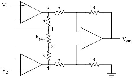
I only use op amps which are single supply and I practically don't use any other op amp except those by Microchip because they're cheap, easy to obtain, and a good number of them have rail to rail I/O. Well, right now I need a single-supply instrumentation amplifier to clean up possible common mode noise from a sensor that'll be located many meters away from the control board. No amplification is necessary or desired. Unfortunately the only IA I have on hand is the INA126 which needs a bipolar supply (else output won't go all the way to ground) and has a minimum gain of 5.
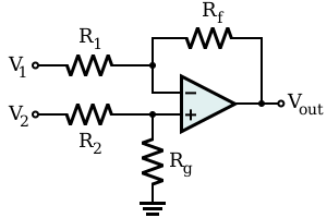
Because the input signal is low impedance I could just use a differential amplifier. I can cobble one up using, say, a MCP6021, but that would entail the hassle of either getting precision resistors or manually matching four. It also increases the parts count. So that got me wondering why Microchip--given their wide range of op amps--hasn't taken the next step and developed instrumentation and difference amplifiers. Do they lack the capability to make these high precision components? Is the demand for these items too small? Is that market cornered by Analog Devices and Texas Instruments?
It's still on my wishlist and hopefully Microchip does get around to fabricating IAs in the near future. I'm sure they'd be more affordable than, say, the AD623.
Because the input signal is low impedance I could just use a differential amplifier. I can cobble one up using, say, a MCP6021, but that would entail the hassle of either getting precision resistors or manually matching four. It also increases the parts count. So that got me wondering why Microchip--given their wide range of op amps--hasn't taken the next step and developed instrumentation and difference amplifiers. Do they lack the capability to make these high precision components? Is the demand for these items too small? Is that market cornered by Analog Devices and Texas Instruments?
It's still on my wishlist and hopefully Microchip does get around to fabricating IAs in the near future. I'm sure they'd be more affordable than, say, the AD623.
Sunday, July 3, 2011
mikroC Pro v4.60 bug
Serendipitiously the mikroC Pro v5.00--successor to v4.60--was just released a couple of days ago. Because I ran into a brick wall programming the PIC12F1822 with the 4.60. The firmware compiled without a hitch for the PIC12F615 but then the compiler started going bananas when I changed the MCU to 12F1822 (had to change the MCU because it turns out I need EEPROM which unfortunately doesn't exist in the 12F615). After systematically commenting out various parts of the program to isolate what was tripping the compiler, I narrowed down the problem to a local variable that the 4.60 demanded be initialized, else it would give me a "362 Not enough RAM 'R15' P12F1822.c" error message upon compilation. Here's an example. The following will result in an error:
I just installed v5.00 and they've apparently fixed this bug. The firmware (still a work in progress) has thus far compiled without the error 362 message popping up.
char i;
void Mozza()
{
char i;
for (i=1; i<8; i++) ;
}
void main()
{
Mozza();
while(1) ;
}
You can change for (i=1; i<8; i++) to something else, like PORTA += i; and the compiler will cough out the same error message. On the other hand, the following versions will compile properly:
char i;
void Mozza()
{
char i=0; // no error if variable initialized
for (i=1; i<8; i++) ;
}
void main()
{
Mozza();
while(1) ;
}
char i;
void Mozza()
{
// char i; no error if global variable is used
for (i=1; i<8; i++) ;
}
void main()
{
Mozza();
while(1) ;
}
So using a global variable or initializing the local var should've been an easy workaround. Unfortunately, when mikroC's built-in EEPROM write functions are present even these tricks fail to lick the problem. I just installed v5.00 and they've apparently fixed this bug. The firmware (still a work in progress) has thus far compiled without the error 362 message popping up.
Subscribe to:
Posts (Atom)