Friday, September 9, 2011

MCU linear regression implementation

Due to noise in the circuit and real-time fluctuations in the phenomenon being measured the readings from a sensor are unsteady and would jump around from millisecond to millisecond just like the day to day up and down variations in the index of trading bourses. However, in the long run the value does show a trend as the variable being measured increases or decreases or remains relatively steady. Thus I'm trying out linear regression--fitting a line through the mess of data points--to tease out this trend. I've used the least squares method since that's what I'm familiar with (actually it's been years and had to hit the math textbooks to refresh my memory!).

What I need to know during every sensor read is the trend at that point. But of course I need some historical readings to compute for it. So I take the last n readings and use those to derive the line of best fit through the n data points. I only need to know the slope of the line (the y-intercept, i.e., the b in ax+b, is irrelevant). If the slope is positive then this implies the value being sensed is increasing, if it's negative it's decreasing, and if it's very close to zero then it's plateaued.

In the application that I have sensor readings are taken at fixed time intervals. The last n sensor readings are stored in an array. During every sensor read the slope is calculated. Because we're always taking the last n readings every time we compute for the slope what we're doing is analogous to computing for a moving average. In this case we can call it a moving linear regression. 

The slope of the line of best fit is given by

(nΣxy - ΣxΣy) / [nΣx2 - (Σx)2]
where

x = point in time
y = sensor reading

y is easy enough to understand. That's just the ADC reading of the analog sensor output. x, as I'm using it here, needs a little more clarification. Let's say our oldest reading of n readings is in cell y[1] and the latest reading is in y[n]. y[i] was taken at time x[i] . But x[i] does not store actual clock time, but rather normalized time. Thus x[1] = 1, x[2] = 2, ...., x[n] = n. The values of x are fixed even as we discard the old y value and shift in the latest. Moreover, the actual time interval between reads isn't or need not be reflected in x as well. Thus the actual elapsed time between two readings may be 5ms, 48ms, 100ms, 2000ms or what have you. As long as that time interval is fixed for all readings then we're good.

Because the values of x never change, the above equation can be greatly simplified. The formula for an arithmetic progression Σx = n(n+1)/2. Hence the least squares equation can be rewritten as

[nΣxy - n(n+1)(Σy)/2] / [nΣx2 - n2(n+1)2/4]

n is common to both the numerator and denominator and so cancel out. We're left with

[Σxy - (n+1)(Σy)/2] / [Σx2 - n(n+1)2/4]

At this point we can provide the firmware the value of n and let it do the calculations, but I'm using an MCU with only 2K of flash. And because I don't want to slow the processor down with unnecessary math computations--whose answers we already know beforehand because n is specified in the defines--I've simplified the formula further still.

Because the 8-bit PICs have very limited RAM and since the rest of the firmware also needs a lot of memory, I settled on n = 15 (I initially tried n = 31 but ran out of RAM). This number is based on the criterion n = 2i- 1, where i = integer, so that n+1 = 2i. The rationale for this constraint is that multiplying by 2i requires nothing more than left shifting the register bits. This reduces computing time and may also reduce code length. With n = 15 the slope of the line simplifies to

[Σxy - (15+1)(Σy)/2] / [Σx2 - 15(16)2/4]

[Σxy - 8(Σy)] / [Σx2 - 960]

Because x = 1, 2, ... n, Σx2 = 1 + 4 + 9 + .... + 225 = 1,240. So the above further simplifies to

[Σxy - 8(Σy)] / [1,240 - 960]

(Σxy - 8Σy) / 280

Keep in mind the above equation is valid only for n = 15. For other values of n the constants will be different.

Here a C implementation of the above equation. It's in mikroC v.5.0.0. Because there are type conversions--integer to floating point and back--it's important to get type casting correctly or you'll get garbage. If in doubt cast the variables explicitly.

Given n = 15, the latest sensor reading is stored in Y[15]. The 15 historical readings are in Y[0] to Y[14]. These 15 values are the ones used in the equation. Y[15] will be copied into Y[14] and used in the next cycle through the state machine (not shown below). Because I want to see the value of the slope, I've added  variable INTSLOPE. To reduce complications of deriving this from the floating point variable SLOPE when it's negative, the firmware computes for (Σxy - 8Σy) such that it's always positive. Because the slope can be and may often lie between -1 and +1, SLOPE is multiplied by 1000 before it's converted to an integer type and stored in INTSLOPE. This provides a resolution of 3 decimal places. For instance if INTSLOPE = 3571 then the actual slope = 3571/1000 = 3.571. The 16-bit INTSLOPE and the sign (plus or minus) of the slope are then transmitted out of the EUSART TX pin so I can view the values on a logic analyzer.


// MCU = PIC12F18xx or PIC16F18xx
// compiler = mikroC v5.0.0
// September 2011


#define  n                   15        // number of data points for linear regression
#define  positive            1         // sign of slope
#define  negative            0         // sign of slope

void LinReg()
{
  unsigned char i;           // counter
  unsigned int Y[n+1];       // newest reading is temporarily stored in Y[n]
                             // and then copied to Y[n-1]
                             // oldest reading is in Y[0] 
  unsigned int SUMY;         // sum of all Y
  unsigned int SUMXY;        // sum of all X*Y
  bit   sign;                // 1 = slope is positive; 0 = slope is negative
  float SLOPE;               // linear regression value of the slope
  unsigned int INTSLOPE;     // integer version of SLOPE. Actually equal to 1000*SLOPE

  Y[n] = CURR;               // CURR = latest sensor reading
  SUMXY = SUMY = 0;
  for (i=0; i<n; i++)
  {
    SUMXY += Y[i]*(i+1);
    SUMY += Y[i];
    Y[i] = Y[i+1];           // discard oldest reading and left-shift all readings including latest one
  }

  SUMY *= 8;
  if (SUMXY >= SUMY)
  {
    SUMXY -= SUMY;
    sign = positive;
  }
  else
  {
    SUMXY = SUMY - SUMXY;
    sign = negative;
  }
  
  SLOPE = SUMXY/280.0;       // this particular equation is valid only for n = 15
                             // SLOPE will always be positive.
                             // Check variable "sign" to determine if slope is negative or positive
  INTSLOPE = SLOPE*1000.0;   
  
  // transmit 16-bit slope and its sign via EUSART
  // EUSART is set up in a separate initialization routine
  while (!PIR1.TXIF);
  TXREG = sign;              // sign byte; 1 = positive slope, 0 = negative slope

  asm {nop}                  // datasheet says TXIF will give false value if read right after loading TXREG
  while (!PIR1.TXIF);
  TXREG = INTSLOPE >> 8;     // high byte

  asm {nop}                  // datasheet says TXIF will give false value if read right after loading TXREG
  while (!PIR1.TXIF);
  TXREG = INTSLOPE;          // low byte
}

----


IMPORTANT ERRATA
September 10 2011

I was fiddling with the circuit and found the following needed to be changed:

unsigned int SUMY;         // sum of all Y
unsigned int SUMXY;        // sum of all X*Y

to

unsigned long SUMY;         // sum of all Y
unsigned long SUMXY;        // sum of all X*Y

16 bits isn't enough when using a 10-bit ADC. SUMXY can exceed 0xFFFF. While Σy will not exceed 16 bits, 8Σy may. So to make sure, I changed both to 32-bit integers.

For a 10-bit ADC, each Y[i] will not exceed 16 bits of course. However, I found out after hours of going nuts that mikroC does not like the following expression/assignment

SUMXY += Y[i]*(i+1);

because, as far as I can tell, it goes bonkers due to the fact that SUMXY is 32 bits while Y[i] is 16 bits and i is 8 bits. To prevent SUMXY from ending up with garbage I had to change the above to

SUMXY = SUMXY + Y[i]*(i+1);

Friday, September 2, 2011

Gear trivia for not so trivial protection

1. All the DMM probes I own have standard exposed metal rods around 2cm long. When doing hot checks on boards or high voltage AC what-have-you I always have to beware of shorting connections and even the probes and such booboos. To minimize inadvertent and unwanted contacts which could have disastrous consequences, I insulated one set of probes with heat shrink tubing, leaving only the conical tip bare. Now they're ultra safe to use.

2. I don't have a purchased ESD wrist strap. I figure I don't need one if the principle is to ground me to earth potential. What I've been using for years now is this. I have a wire that's connected to a copper stake that's been driven into the soil (earth). A 1 Mohm resistor is soldered in series. This resistor limits the current that may possibly go through you know who. At the other end of the wire is an alligator clip. Since I don't particularly like gators biting me, I wear my watch which has a metal strap to which I clip the alligator onto. When not using it on my wrist, the alligator clips onto a metal sheet I have on the bench. When I can't find my watch or am just too lazy to even put it on, I touch and wipe my hands on the sheet every so often and hope to Thor I won't zap any ICs.

Tuesday, August 30, 2011

Taking a peek at RS-485 signals

Did a test of RS-485 lines. See the schematic for the transmitter section of the circuit. Three SN75176B transceivers were employed. One was configured as driver (transmitter), two as receivers. Driver was on only when transmitting. Vcc was cut off when not transmitting. Transmitter and receivers were connected using Samsung 4-pair AWG24 Category 5 UTP cable. Cable length from transmitter to the farthest receiver was around 30 meters. One pair was used for RS-485 line A and B, two pairs for power supply to the transmitter. The test receiver used below had its own power supply but all transceivers shared a common ground. There were no termination resistors across lines A and B. Pullup and pulldown resistors were as per schematic--20kohms each. Data packet consisted of 4 bytes + a 9th bit. Minimum time interval between packet transmission was ~50ms. Baud rate was 19.2 kbps.

In the following screenshots,
Channel 1 (yellow) = Line A
Channel 2 (cyan) = Line B
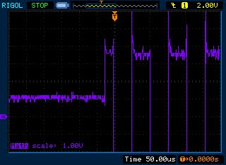
Math channel (purple) = A - B

Overshoots and undershoots are clearly visible during high/low transitions. In all probability these are due to signal reflections in the cable.


Zooming in:


With math channel turned on:


Channels 1 and 2 are turned off and vertical scale of math is decreased from 5 to 2V/division:


Vertical scale reduced to1V/div. Look at the left half of the trace. When transmitter is off A - B is approximately 1.0V. (Adjusting the vertical scale to <1V/div and using cursors, I was able to take a more accurate reading of 1.08V. With only one receiver connected A-B = 1.50V). Since this is >200mV pin R of the receivers will be high--the mandatory and expected line idle state.


Here are zoomed in views of over- and undershoots. The ringing dies out well before half a bit width. The first screenshot shows line A going from low to high. The second shows line A going from high to low. Note the different horizontal scales--500ns in the first, 200ns in the second.


My Rigol scope only has two channels so in the following screenshots
Channel 1: Line A
Channel 2: SN75176B pin R


Even with the ringing there are no errors in the output of the receiver, although undershoot does occur occasionally in pin R output (the Rigol is prone to aliasing, so there may in fact be very high frequency ringing which isn't showing up at this horizontal scale.)

With horizontal scale reduced, we get to see details of undershoots on pin R.


Overshoots when pin R goes from low to high are probably less frequent--I haven't been able to capture any yet.


Just to be fair to line B I let 
Channel 1: Line B
Channel 2: SN75176B pin R


What I'd like to do in the future is to increase the baud rate to >100kbps and increase the cable length. Should be interesting to see how bad the ringing will get. And how it will affect data integrity. Something like the following is expected.


That's from a lab test performed by Texas Instruments. Baud rate was 200kbps. 100 feet of Bertek 100-ohm AWG24 twisted pair cable was used. There was one driver and only one receiver (TI AM26C31C and AM26C32C).

Sunday, August 28, 2011

Using RS-485 transceivers

The beauty of using RS-485 (more formally known as the TIA/EIA-485 standard) for long distance serial communication is that because it uses differential lines it's largely immune to common mode voltages and noise. It's also utterly simple electrically--at least in a half duplex setup--in that it uses only one twisted pair cable and a common ground.

Here's a setup for perhaps the simplest possible configuration: there's only one transmitter and one or more receivers. In other words communications is a simplex type--information goes only one way. The transmitter sends out data while the receivers intercept the data stream but do not transmit anything.


In the above circuit the non-inverting input of the unity gain buffer is connected to a sensor circuit with an analog output. The MCU's ADC converts the sensor reading to a digital value and sends it out serially. U1 is a RS-485 transceiver. Pin DE and /RE are controlled by the MCU, switching them high only when transmitting.

At the heart of the RS-485 is the transceiver. In fact RS-485 is merely an electrical standard. And the particular electrical characteristics of the transceivers determine whether one has a RS-485 circuit or not. There are a lot of transceivers out there and I would rather use something like Maxim's MAX48x series, but the price is simply eye popping! They're as expensive as instrumentation amplifiers. Instead I've been using the jurassic SN75176B which is over five times cheaper. Texas Instruments says it's rated for 10Mbps throughput. But hey my requirements are 2 to 3 orders of magnitude lower.

The problem with the 757176 is that it's a gas guzzler. An informal test shows that it draws some 16mA @Vcc = 5V when it's set up for reception only (pins DE and /RE are low). This shoots up to around 32mA when it's in transmission mode (pins DE and /RE are high). As Dave Jones would say, you can fly to moon on 32mA!

To limit the amount of juice it gulps, we can--at least in a simplex arrangement--turn off the 75176 when no transmission is being performed. As can be seen in the schematic above, a PNP transistor is used to power it up/down. When transmission of a data packet is about to commence the transceiver is switched on and right after the last stop bit is sent, the 75176 is powered down. Average power consumption of the transmitter circuit will depend on how frequent transmissions are made. It will also depend on the baud rate--the higher, the less time every transmission takes and therefore the shorter the time the transceiver will be on.

In half duplex systems where drivers (transmitters) are also receivers powering down the transceiver will probably be not an option.

A very important issue with these transceivers is to ensure that they will be fail-safe. Fail safe in this context means that even if the transmitter's DE pin is grounded--ie., the driver is disabled and lines B and A become tri-stated to high impedance--or if power to the transmitting transceiver is cut off as it is in the circuit above--any and all the receivers will still see a differential voltage between B and A that's > 200mV. As per the RS-485 standard, if -200mV < B - A < +200mV, then output of pin R will be indeterminate. To guard against this bias resistors are added to lines A and B. In the schematic above these are pull-up resistor Rb1 and pull-down resistor Rb2.

Very important note: The RS-485 standard states that when the difference between the voltages between B and A is > +200mV (i.e, B - A > 200mV) then a logic 1 is output on the receiver, and when B - A <. -200mV then a logic 0 is output. But chip manufacturers like Texas Instruments and Maxim have reversed this. And so B is A and A is B on their transceivers. No problem as long you don't mix transceivers that use the RS-485 standard labeling. From hereon I'll follow the TI / Maxim convention. 

The values of the bias resistors determine the differential voltage A - B. How much bias resistance should be installed depends on how many receivers are connected to the network. For the transceiver used above, each receiver has a minimum input resistance of 12Kohms. The more receivers there are the less the total resistance there is since the input resistances are in parallel. This translates to lower value bias resistors. Here's how to compute the values:

Let:
Ritotal = total input resistance
I = current through Ritotal
VCC = power supply voltage to which pull-up resistor will be connected
Rb = bias resistor value
RT = total resistance which includes the bias resistors and Ritotal

We require that the voltage across the total input resistance be greater than 200mV:

I Ritotal > 200mV

Solving for current:

I > 200mV / Ritotal

The bias resistors and Ritotal are in series and form a voltage divider and we define their sum as the total resistance:

RT = 2Rb + Ritotal

It's also equal to:

RT = VCC / I

Since we're looking for the value of the bias resistors:

Rb = (RT - Ritotal)/2

Substituting and simplifying we obtain:

Rb < (5VCC - 1)Ritotal / 2

Example: Let's say we have two SN75176B transceivers on the network configured as receivers. VCC = 5V. Each transceiver has an input resistance of 12Kohms. Because they're in parallel, Ritotal = 6K. Using the formula above, we find that bias resistors should be less than 72Kohms each in order for A - B to be > 200mV when transmitter is disabled (lines A and B are in a high impedance state).

If termination resistors are present then total resistance would be = Ritotal|| termination resistors. So if two 120 ohm termination resistors were present (termination resistors are usually between 120 and 150 ohms when using UTP cables) and the Ritotal= 6K then the total resistance = 6K || 120 || 120 = 1/(1/6000 + 1/120 + 1/120) = 59.4 ohms. Computing for the bias resistors we obtain 720 ohms. Because the very low resistance values of termination resistors, as much as possible we don't want to install them since they significantly increase power consumption.

Termination resistors are used across lines A and B for impedance matching to prevent/minimize signal reflections leading to ringing. So when do we need termination? Well, it depends if we have a short or long line/cable. One heuristic for determining whether a line is long or short is as follows.

Let:
tt = transition time also known as rise/fall time of transceiver's transmitter signal in seconds
RP = propagation rate of electrical signals in copper = 0.2m/ns = 2 x 10⁸m/s
L = cable length in meters

A line is considered long if:

tt < 2(L/RP)

(see Maxim's equation for a more conservative figure).

According to the SN75176B datasheet its tt = 20ns. Let's solve for L to see how long the cable can be before it's deemed long.

L = ttRP/2 = (20 x 10-9)(2 x 10⁸)/2 = 2 meters.

So if we're using the SN75176B and our cable is longer than 2 meters termination resistors are necessary. That's not the end of the story, however. We may still be able to get away without having any termination even at cable lengths much longer than this:
If the rise time is unknown, another way of deciding whether a line is long or short is to compare the shortest expected bit width and the 1-way cable delay. This method considers two factors: the reflections may bounce back and forth several times before settling, and the bit rates at the transmitter and receiver may vary slightly from each other. As a general guideline, if the bit width is 40 or more times greater than the delay, any reflections will have settled by the time the receiver reads the bits. (Axelson, p.111)

The key to obviating the need for termination is to have a sufficiently slow baud rate so that reflections in the transmission line (a "long line") have already died out by the time the microcontroller reads the bit. The 1-way cable delay is merely L/RP. Thus for a 100-meter wire, the 1-way cable delay = 500ns or 0.5µs. Using the above guideline we can determine the maximum cable length given a particular transmission baud rate--the bit width is the reciprocal of baud rate.

Let:
B = transmission baud rate in bits/sec
RP = propagation rate of electrical signals in copper = 0.2m/ns = 2 x 10⁸m/s
L = cable length in meters

The guideline states that:

1/B >= 40(L/RP)

Solving for L we have:

L <= [(1/B)/40]RP

L <= RP/(40B)

For a baud rate of 19,200, L = 260 meters. So theoretically no termination is necessary if cable length is less than this. Just out of curiosity let's see the maximum baud rate at which we can transmit for the 2-meter cable above.

B = RP/(40L) = 2.5Mbps


----

References:

Janet Axelson, Serial Port Complete: COM Ports, USB Virtual COM Ports, and Ports for Embedded Systems, 2ed, Lakeview Research LLC, 2007, Chapters.6 & 7.

Polarities for Differential Pair Signals (RS-422 and RS-485)


RS-422 and RS-485 Application Note (computation of bias resistor values)

AN1090 Methods for Trimming the Power Required in RS-485 Systems

Wednesday, August 17, 2011

ADC LSb mystery

Does a 10-bit ADC really have a resolution (not accuracy) of 10 bits? Apparently it might not. I've been having problems with the LSb (least significant bit) of the ADC output of PICs. What's happening is that even with a stable, fixed-voltage input signal to the ADC, the digitized output--depending on the VDD level and the input voltage signal--may either be stable or the value flip flops between two values (one LSb apart) from one conversion to the next.

The LSb problem is dependent on both VDD and ADC input signal level. For example the problem might not occur at input signal X volts with a VDD = 4.950V but will appear when VDD is within the range of 3.0 to 3.6V. And/or it might get worse (i.e., the number of times the LSb changes becomes more frequent) as one approaches a certain voltage range. Or for a certain signal voltage Y, the problem may be nonexistent at all with VDD from 2.5 to 5.0V. Or for signal Z the the LSb glitch may be present at practically the entire operating voltage range of the MCU/ADC.

I've tried everything I can think of to get rid of this hair-tearing problem: I've used a linear power supply instead of a switchmode to minimize power supply noise. I've used separate power and ground lines for digital and analog and employed star connections. Actually digital noise should be minimal since, as we'll see, the MCU goes to sleep when the ADC is reading. I've also peppered the circuit with filter and bypass caps. The circuit is in open air but I still allowed it to settle down thermally so drifts due to temperature are eliminated. I admit the circuit is breadboarded and not soldered onto a PCB and so contact problems may be the culprit. To minimize that possibility I've used redundant connections. I also tried buffering the voltage signal using an op amp. Though there has been a reduction, the above solutions have not completely eliminated the problem.

Here's the test circuit:


Bridge rectifier output is approximately 12VAC. Potentiometer is a 5-ohm multi-turn Bourns 3590S-2-502L. Because this is the only highly reliable pot that I have and because output voltage of the LM317 must not exceed 5V (the PIC's max VDD ), I had to add the 560 and 220 ohm resistors. When the pot is turned all the way to zero, the 560 ohm resistor is shunted leaving only the 220 ohms. When the pot is at its maximum 5K, it's in parallel with the 560 giving a net resistance of 504 ohms. This in turn is in series with the 220 ohm, giving a total of 724 ohms. Plug those values into the LM317 equation and the effective output range of this power supply is 2.4 to 5.0V.

Firmware is as follows. It's the 3rd or 4th revision. The ADC uses VDD as its positive reference and ground as its negative voltage reference. Thus the ADC output will be ratiometric with respect to the power supply. This way the analog to digital conversion is immune to drifts in the power supply. ADC read is performed approximately every 8ms. Because the PIC12F1822's ADC has silicon flaws, ADC read is performed during sleep, thus although timer0 tick is set to 8ms, several hundred microseconds are added while the system clock is shut down. The ADC read takes so long because there are actually two sets of reads. One is a single read and the other is a set of 16 reads which are then averaged. I tried averaging the reads to see if I could get obtain a value that doesn't keep flipping around. After the reads, the current and previous reads are compared. If they're different then the corresponding MCU pins (neflag and neflagave) are made high, else they're made low. Those pins are connected to an oscilloscope and logic analyzer so I can see how (un)stable the ADC reads are. In this final revision of the firmware I've also enabled the EUSART so I can see by how many bits the ADC reads differ (the Saleae Logic analyzer automatically decodes the serial data stream). Only the lower byte of the ADC output (register ADRESL) is transmitted.


/*

processor = PIC 12F1822
compiler = mikroC Pro v.5.0.0
August 2011

Test of ADC LSb 
 
internal oscillator is used, WDT disabled, power up timer and brown out reset disabled, MCLR disabled

*/


#define  neflag              PORTA.f5            // not equal flag; 1 = previous and current ADC values are not equal
#define  neflagave           PORTA.f4            // not equal flag average; 1 = previous and current averaged ADC values are not equal
#define  t0ini               256 - 250           // value loaded into TMR0 every time it overflows


void IniReg()
{
  OSCCON    = 0b1101000;     // internal clock 4Mhz
  TRISA     = 0b100;
  ANSELA    = 0b100;
  PORTA     = 0;

  TMR0      = t0ini;
  OPTION_REG = 0b10000100;   // Weak pull ups disabled
                             // timer0 uses internal clock,
                             // prescaler assigned to timer0, prescaler = 1:32

  ADCON0 = 0b1001;           // channel 2, ADC on
  ADCON1 = 0b11110000;       // right justified, use Frc, Vdd as positive reference voltage
  INTCON.GIE = 0;            // global interrupt disabled
  PIE1.ADIE = 1;             // ADC interrupt enabled

  // baud rate = 2400
  SPBRGH = 0;
  SPBRGL = 25;
  RCSTA.SPEN = 1;
  TXSTA.TXEN = 1;
  TXSTA.SYNC = 0;

} // void IniReg()


/* =========================================================================================================

According to PIC12F1822 Silicon Errata sheet DS80502C the ADC unit in certain silicon revisions is buggy:

"Under certain device operating conditions, the ADC conversion may not complete properly.
When this occurs, the ADC Interrupt Flag (ADIF) does not get set,
the GO/DONE bit does not get cleared and the conversion result
does not get loaded into the ADRESH and ADRESL result registers."

mikroC Pro v5.00 compiler's Adc_Read() built-in ADC function uses the GO/DONE bit to check conversion completion (without putting the MCU to sleep, of course)
so the function cannot be used. And indeed the MCU hangs (when WDT is disabled) or the MCU resets when WDT is enabled.

The workaround used here is as per method 1 in the said errata:

"Select the dedicated RC oscillator as the ADC conversion clock source,
and perform all conversions with the device in Sleep."

=========================================================================================================  */

unsigned int ADC()
{
  PIR1.ADIF = 0;                       // clear ADC interrupt flag
  INTCON.PEIE = 1;                     // peripheral interrupts enabled
  ADCON0.GO = 1;                       // start ADC conversion
  asm {sleep}                          // zzzzzzzzzzzzzzz.... when ADIF = 1 MCU will wake up and will continue execution of the program
  PIR1.ADIF = 0;                       // clear ADC interrupt flag
  INTCON.PEIE = 0;                     // disable peripheral interrupts
  return ADRESH*256 + ADRESL;          // return the 10-bit ADC value as a 16-bit number
}

void Compare()
{
  unsigned char i;
  static unsigned int CURR = 0;        // current single ADC reading
  static unsigned int CURRAVE = 0;     // current average of 16 ADC readings
  static unsigned int PREV;            // previous single ADC reading
  static unsigned int PREVAVE;         // previous average of 16 ADC reading
  unsigned int SUM;                    // sum of 16 ADC readings

  PREVAVE = CURRAVE;
  SUM = 0;
  for (i=0; i<16; i++)
    SUM += ADC();

  PREV = CURR;
  CURR = ADC();
  
  TXREG = CURR;                        // bec ADC is performed during sleep while serial data transmission is dependent of the system clock
                                       // transmission can only begin after all ADC reads are done

  if (CURR == PREV)
    neflag = 0;
  else
    neflag = 1;

  CURRAVE = SUM / 16;
  if (SUM % 16 >= 8)                   // number rounding algorithm
    CURRAVE += 1;

  if (CURRAVE == PREVAVE)
    neflagave = 0;
  else
    neflagave = 1;
}

void main()
{
  IniReg();

  while(1)
  {
    if (INTCON.TMR0IF)
    {
      TMR0 = t0ini;
      Compare();
      INTCON.TMR0IF = 0;
    }
  } // while(1)
} // void main()


I used the oscilloscope with time base on roll mode with one channel monitoring neflag and other neflagave. I opted not to take screenshots of the scope--would take too much effort. But here are some of the logic analyzer data at particular voltages. As you can see the averaging routine sometimes works, sometimes doesn't, depending on how bad the LSb problem is. Resistor values are as per their color code. VDD values are actual measured voltages using a Fluke 87V.

I. Ra = 5.1K, Rb = 4.3K

A. VDD = 2.502V


B. VDD = 4.000V


C. VDD = 5.000V


II. Ra = 5.1K || 330 = 310, Rb = 4.3K


I provide only a screenshot for VDD = 5.000V. There is absolutely no LSb problem for VDD = 2.5V to 5.0V


III. Ra = 5.1K, Rb = 4.3K || 330 = 306

A. VDD = 2.999V


B. VDD = 3.499V


C. VDD = 4.500V


D. VDD = 5.000V


So what could be causing this ADC read glitch? Well, no ADC is 100% accurate. It will have various sources of errors--among them INL, DNL, offset, and gain errors--due to silicon and its fabrication. But accuracy isn't our problem; it's resolution. Ostensibly none of these is the error that I've encountered. What it does look very much like is conversion error due to transition noise, also known as code-transition noise or code-edge noise. Transition noise is,
the range of input voltages that cause an ADC output to toggle between adjacent output codes. As you increase the analog input voltage, the voltages that define where each code transition occurs (code edges) are uncertain due to the associated transition noise.

Keeping the input signal constant and performing lots of ADC reads, the distribution of ADC output codes is supposedly Gaussian (normal distribution). In the tests with the PIC, however, apparently there are only two codes, i.e, output varies by only one LSb. I haven't done it, but it should be easy to have the MCU read a thousand or ten thousand times and tell us whether the codes vary by more than one LSb.

Interestingly, averaging, which I used in the firmware above, is the recommended algorithm to address LSb flickering. However, as we've seen even averaging (at least the way it was implemented above) isn't a panacea. Maybe I'm doing it wrong.

Wednesday, July 27, 2011

Is it dawn yet? How shall we know?

Those of you who've been following the development of the MCU-based ANLC will probably remember that I turned to a micrcocontroller since I want to switch the load off not at the ambient light level (corresponding sensor voltage) at which we want to turn on the load, nor at the load turn-on ambient light level + some hysteresis, but rather at the very crack of dawn, which corresponds to a light level significantly less than that at load turn-on. So you might be wondering what algorithm I'm currently using to implement that.

With all other factors (clouds, city lights, etc.) kept constant, one characteristic of dawn is that the light level rises evenly and continuously (thanks to the very stable rotation speed of the earth and nearly constant light output of the sun). And this increase will not exceed a certain dV/dt--which we've measured (at least in my particular location in the globe which happens to be 15° north of the equator) to be almost 6mV/s (@Vdd = 5V).

So one way of ruling out other light sources is to look at whether dV/dt > 0 but < 6mV/s and whether this is sustained over time. If it's currently very dark (night time) and these conditions are met then there is a good probability we are witnessing dawn/sunrise. If not then there is a good chance the light source isn't the sun.

In addition we'd want to monitor for the above conditions as close to actual dawn as possible. We don't, for instance, want to check after just a couple of hours after dusk. And speaking of time of day, our circuit doesn't actually know what time of day it really is. For instance just because ambient light level has dropped below the trip point doesn't mean it really is dusk. It may be midday but the sky is so heavy with dark nimbus clouds that the light level has dipped to a point that the load has been turned on. The algorithm needs to take this into consideration.

One way of gaining confidence that it really is nighttime is to monitor the amount of time the load has been on. If the shortest night during the entire year is, say 10 hours, then we can be fairly sure that it's night if the load has been on for at least 8 hours. We can thus wait 8 hours after the load has been on before beginning to check for dawn conditions.

We can also monitor the sensor voltage to find out if it's really nighttime, but the night time reading/value will depend on where we install the sensor and how much artificial light sources will be polluting it. As I mentioned before I placed the sensor on the roof and shielded it on the sides to minimize the effects of streetlights, billboard lights, et al.

Besides just waiting x hours to begin monitoring for dawn dV/dt, we also want to find out the maximum light level for an hour or two before the time we begin checking for dawn because we only want to start applying our dawn dV/dt criteria when ambient light level exceeds this value. Given that this is the maximum ambient light level close to dawn, there is a greater probability that light whose intensity exceeds it and which keeps increasing but has a rate of increase less than the max dV/dt is in fact indicative of the first rays of the sun trickling in and not some other light source.

While I've implemented the above set of detection conditions for several days now--and so far so good--I imagine they do not provide a foolproof way of determining the onset of dawn. For example, if our firmware is already monitoring for dawn conditions and clouds begin rolling in, gradually reflecting more of the city lights thus increasing the sky light level and if the clouds move in at just the right rate so that max dV/dt isn't exceeded, then our firmware will be fooled into switching the load off.

One way of further improving the system is to add another sensor. We set the sensors up such that one receives light mainly from the eastern part of sky while the other from the western half (this can be as simple as having the LDRs side by side with an opaque board between them to block light from the eastern/western side of the sky from falling on the west/east LDR). We can then monitor for differences in light levels detected. Surely the eastern part of the sky will be brighter at dawn. As a bonus we can use this setup to detect dusk as well.

For now, however, I'm sticking to a simple single-LDR sensor. There won't be need to make it any more complex if the algorithm works or a better algorithm can improve dawn detection.

Monday, July 25, 2011

A more decent measurement of dawn and dusk dV/dt

I previously estimated the maximum dV/dt of the MCU-based ANLC sensor during dusk and dawn at 4.5mV/s, but I want to have a more accurate figure. Because I don't have the proper test gear, I had to make do with a DMM and a stopwatch.

I decided to keep dV constant at 0.1V and record the time it took for the sensor voltage to increase/decrease by that amount. Thus what I was recording was in fact dt/dV. It would then be a simple matter of getting the reciprocal to obtain dV/dt.

The stopwatch of my Nokia cell phone has a "split timing" feature that allows the user to press the button and have a reading without actually stopping the stopwatch. Unfortunately, while using it I found out that it has a limit of 20 split timing readings. So as you will see, there are breaks in the data and graph. Those are the times when I had to reset the stopwatch. Too bad I just discovered this online split timer and countdown timer. Would've been great to use it.

The July 23 readings were a spur of the moment thing. I didn't actually plan to record the values. And so data on that date are quite limited.

Enough intro. Here's the spreadsheet with all the data, computations and graphs.


It's clear from the table and graphs that the maximum dV/dt is almost 6mV/s. Two things of interest: 1. The curves for dawn and dusk apparently don't have the same shape. Wonder if more data will even out the differences or if this difference is intrinsic. 2. The July 24 dusk graph is shifted downwards compared to the previous day's. This is probably because it was rather overcast on the 24th. That dV/dt can be attenuated by cloud cover needs to be noted.